
qixinwei-pcba


XC7Z100-1FFG900I AMD (Xilinx) Zynq-7000 SoC Dual-Core ARM Cortex-A9 444K Logic Cells 362 I/O 16 GTX 900-FBGA Industrial
XC7Z100-1FFG900I Product Overview
The XC7Z100-1FFG900I is a System-on-Chip (SoC) from AMD (formerly Xilinx), part of the Zynq-7000 family, housed in a 900-pin FBGA (FFG900) package and manufactured using 28nm process technology. The device integrates a dual-core ARM Cortex-A9 MPCore processor (up to 667MHz, -1 speed grade) with Kintex-7 programmable logic resources, providing 444K logic cells and 26.5Mb of Block RAM, featuring 362 user I/O pins. The chip incorporates 16 GTX high-speed transceivers, each running at up to 12.5Gbps, and rich interface resources including dual Gigabit Ethernet, USB 2.0, SD/SDIO, UART, SPI, I2C, and CAN, with DDR3 memory controller support. It operates over an industrial temperature range of -40°C to +100°C with speed grade -1, delivering high-performance processing and flexible programmable logic expansion for industrial control, embedded vision, automotive electronics, and communication equipment applications. XC7Z100-1FFG900I is a versatile and dependable SoC.
XC7Z100-1FFG900I Core Features
Processor System: Dual-core ARM Cortex-A9 MPCore, up to 667MHz, with NEON SIMD and double-precision floating-point unit
Programmable Logic: 444K logic cells (Kintex-7 equivalent), 277.4K LUTs, 554.8K flip-flops, 26.5Mb Block RAM
User I/O: 362 user I/O pins supporting various single-ended and differential standards
High-Speed Transceivers: 16 GTX transceivers, each up to 12.5Gbps
DSP Capability: 2020 DSP Slices for efficient digital signal processing
Memory Interface: Supports DDR3, DDR3L, DDR2, and LPDDR2, up to 1066Mb/s
Peripheral Interfaces: Integrated dual Gigabit Ethernet, USB 2.0 OTG, SD/SDIO, UART, SPI, I2C, CAN
Operating Conditions: Core voltage 1.0V, I/O voltage 1.2V-3.3V, industrial -40°C to +100°C
Package: 900-pin FBGA (31x31mm), surface mount, RoHS compliant
XC7Z100-1FFG900I is designed for robust performance.
XC7Z100-1FFG900I Applications
Industrial Control: XC7Z100-1FFG900I can be used in industrial Ethernet, motion control, and PLC systems for real-time data processing and communication.
Embedded Vision: XC7Z100-1FFG900I supports image sensor interfaces, image pre-processing, and feature extraction for smart cameras and machine vision.
Automotive Electronics: XC7Z100-1FFG900I is suitable for advanced driver assistance systems (ADAS), infotainment, and body control.
Communication Equipment: XC7Z100-1FFG900I is suitable for small base stations, remote radio units, and network protocol processing, with 16 GTX transceivers supporting multi-channel high-speed serial connectivity.
Medical Devices: XC7Z100-1FFG900I can be used in portable medical monitors, ultrasound imaging, and signal processing.
IoT Gateways: XC7Z100-1FFG900I integrates processor and FPGA, suitable for edge computing, protocol conversion, and data aggregation.
XC7Z100-1FFG900I Key Advantages
Processor and FPGA Integration: Single-chip integration of dual-core ARM Cortex-A9 processor and Kintex-7 FPGA reduces board space and system complexity.
Integrated High-Speed Transceivers: Built-in 16 GTX transceivers at 12.5Gbps eliminate external PHY chips for multi-channel high-speed serial communication, suitable for communications and video applications.
Rich Peripherals: Built-in dual Gigabit Ethernet, USB 2.0, and other high-speed interfaces reduce external chip requirements and BOM cost.
Flexible I/O Support: 362 user I/O pins support DDR3 interfaces and multiple level standards, adapting to various peripherals and bus protocols.
Mature Development Ecosystem: Supports AMD (Xilinx) Vivado and Vitis development tools, with rich IP core resources to accelerate product development.
Industrial-Grade Reliability: Operating temperature range of -40°C to +100°C meets demanding industrial and outdoor requirements.
Why Choose QIXINWEI
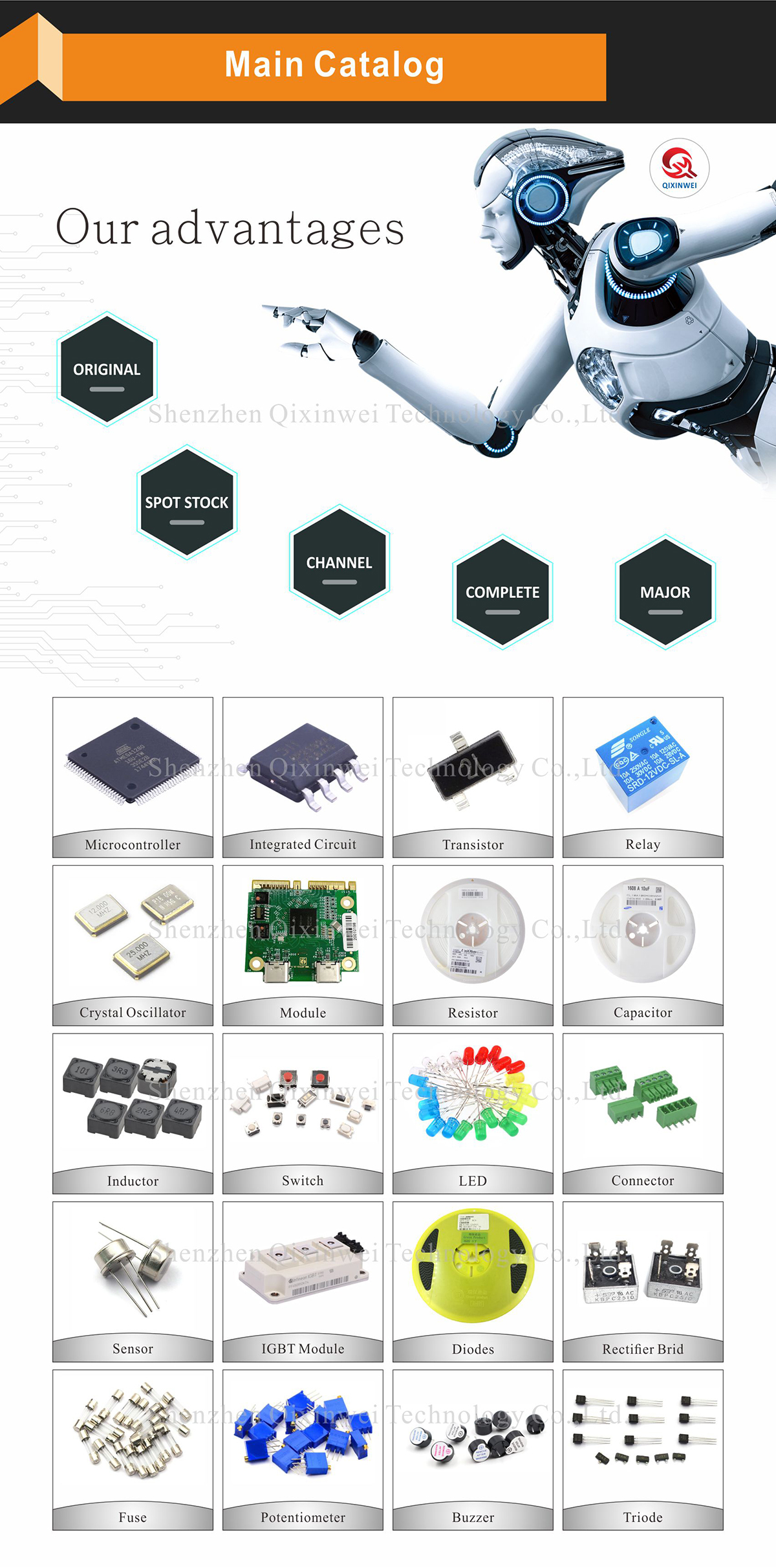
Years of experience in the electronics industry. Trusted by global customers.
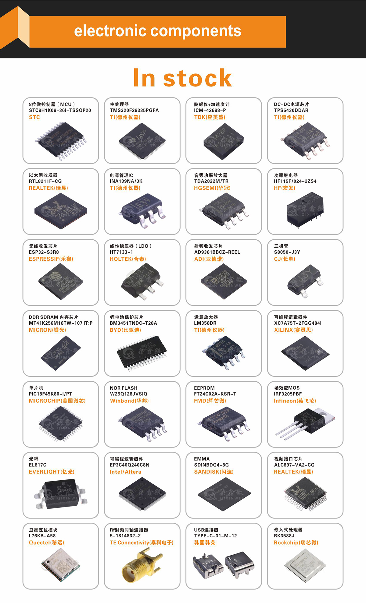
Massive In-Stock Inventory – Ready to ship promptly.
BOM Matching Service – One-stop solution, save time.
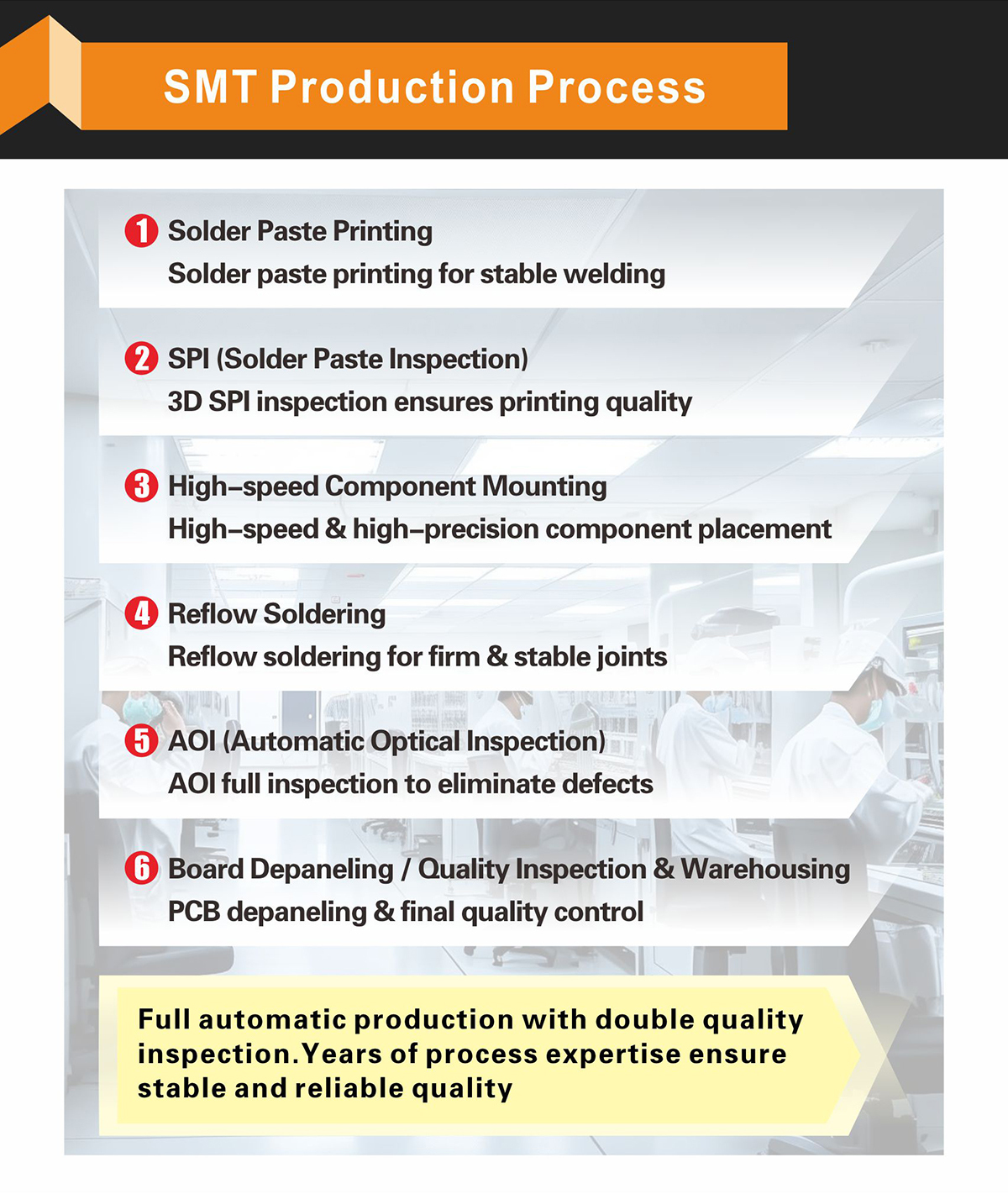
PCBA Customization – Professional engineering team creates tailor-made solutions based on your needs.
Cost-Effective & Efficient – Better channel, better cost.
A dedicated team makes your procurement smoother.
Contact us for BOM quotes or PCBA inquiries.








FAQ
- Is XC7Z100-1FFG900I an FPGA or a processor?
- XC7Z100-1FFG900I is a Zynq-7000 series SoC that integrates a dual-core ARM Cortex-A9 processor and Kintex-7 programmable logic, offering both processor and FPGA capabilities.
- What is the performance of the built-in ARM processor?
- It integrates a dual-core ARM Cortex-A9 MPCore with a maximum frequency of 667MHz (speed grade -1), supporting NEON SIMD and double-precision floating-point operations, suitable for Linux or bare-metal applications.
- How large is the programmable logic portion?
- It provides 444K logic cells, 277.4K LUTs, 554.8K flip-flops, 26.5Mb Block RAM, and 2020 DSP Slices, suitable for large-scale logic design and signal processing.
- How many high-speed transceivers does this chip have? What is the rate?
- It integrates 16 GTX high-speed transceivers, each capable of up to 12.5Gbps, suitable for optical communications, PCIe data links, and multi-channel high-speed serial interfaces.
- What external memory interfaces does it support?
- It supports DDR3, DDR3L, DDR2, and LPDDR2 memory with data rates up to 1066Mb/s, meeting embedded system memory requirements.
- What interface standards do the 362 I/O pins support?
- It supports various single-ended and differential standards, including LVTTL, LVCMOS, SSTL, and LVDS, with I/O voltage range 1.2V to 3.3V.
- What high-speed peripheral interfaces does this device support?
- It integrates dual Gigabit Ethernet, USB 2.0 OTG, SD/SDIO, UART, SPI, I2C, CAN interfaces for industrial communication and connectivity.
- What tools and software are needed for development?
- Use AMD (Xilinx) Vivado for FPGA design and Vitis for software development and system integration, supporting PetaLinux and bare-metal development.
- Hardware debugging can be performed via JTAG interface for in-circuit configuration and debugging.
- What does the -1 speed grade mean?
- The Zynq-7000 series offers -1, -2, and -3 speed grades, with -1 being the base speed grade, providing processor frequency up to 667MHz, suitable for most industrial and commercial applications.
- What is the operating temperature range of this chip?
- The industrial temperature range is -40°C to +100°C (junction temperature), suitable for industrial automation, outdoor communication equipment, and harsh environments.
- Property:
- Specification
- Product Type:
- System-on-Chip (SoC)
- Brand:
- AMD (formerly Xilinx)
- Series:
- Zynq-7000
- Processor:
- Dual-core ARM Cortex-A9 MPCore, up to 667MHz
- Logic Cells:
- 444K
- LUTs:
- 277.4K
- Flip-Flops:
- 554.8K
- Total RAM Bits:
- 26.5Mb Block RAM
- User I/O:
- 362
- High-Speed Transceivers:
- 16 GTX, up to 12.5Gbps
- DSP Slices:
- 2020
- Speed Grade:
- -1
- Core Voltage:
- 1.0V
- I/O Voltage:
- 1.2V - 3.3V
- Operating Temperature:
- -40°C to +100°C (Industrial)
- Package:
- 900-FBGA (31x31mm)


