STM32F103ZET6 development board, ARM Cortex-M3, 72MHz, 512KB Flash, 64KB RAM. Onboard crystal, reset button, power LED, all 144 pins broken out. Ideal for embedded learning, industrial control, IoT, robotics, graduation projects. Arduino IDE compatible
STM32F103ZET6 Development Board Application features:
◆ Main Chip
STM32F103ZET6
◆ Core Architecture
ARM Cortex-M3
◆ Clock Speed
72MHz (maximum)
◆ Memory
Flash: 512KB
SRAM: 64KB
◆ Debug Interface
SWD / JTAG (20-pin standard)
◆ Onboard Resources
8MHz crystal
32.768KHz RTC crystal
Reset button
Power indicator (PWR)
User LED (PC13)
Micro USB / Mini USB (power)
◆ Pin Headers
All 144 pins broken out (2.54mm pitch)
◆ Communication Interfaces
USART ×5 / I2C ×2 / SPI ×3 / CAN ×2 / USB 2.0 / SDIO
◆ Peripherals
ADC ×3 (16 channels) / DAC ×2 / Timers ×8 / PWM
◆ Typical Applications
Embedded system learning
Industrial control equipment
IoT nodes
Robotics control
Graduation projects / competitions
Smart home
Data acquisition systems
◆ Key Advantages
Classic Cortex-M3 core
All 144 pins accessible
Rich resources (512KB Flash)
Compatible with Standard Lib/HAL Lib/Arduino
Abundant tutorials and examples
Great for beginners and project development
Why Choose QIXINWEI
Years of experience in the electronics industry. Trusted by global customers.
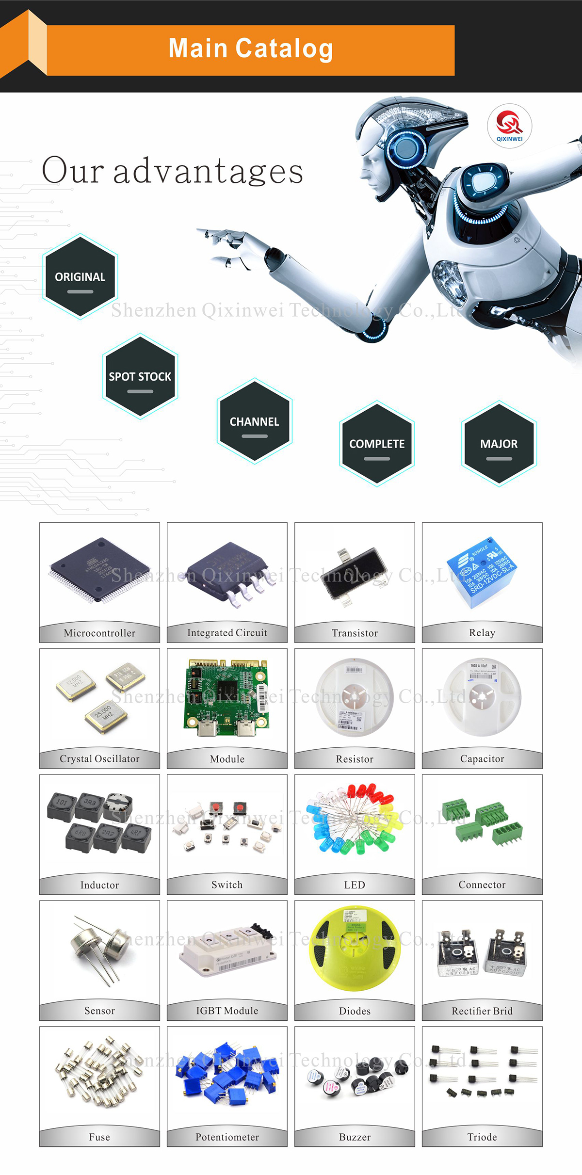
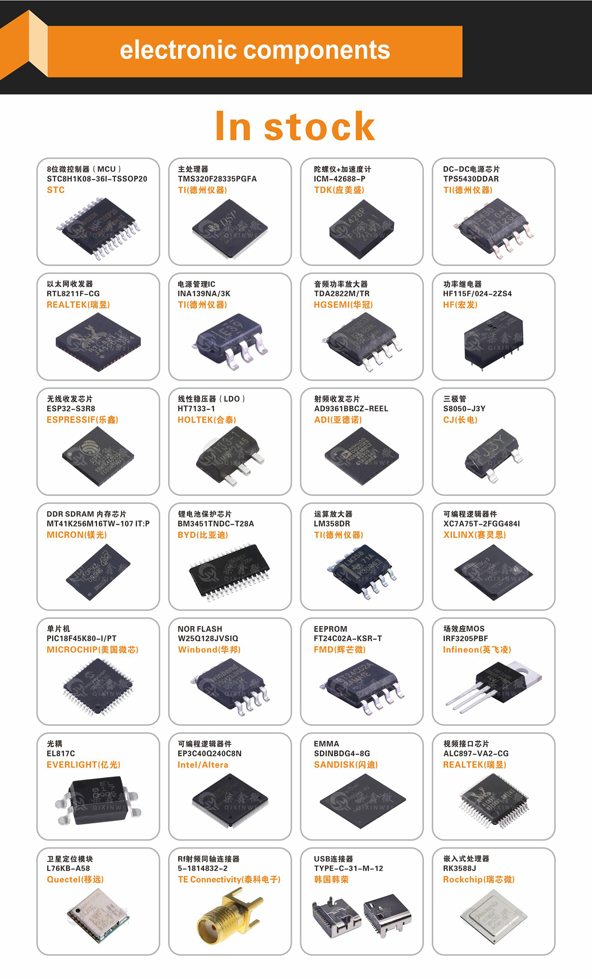
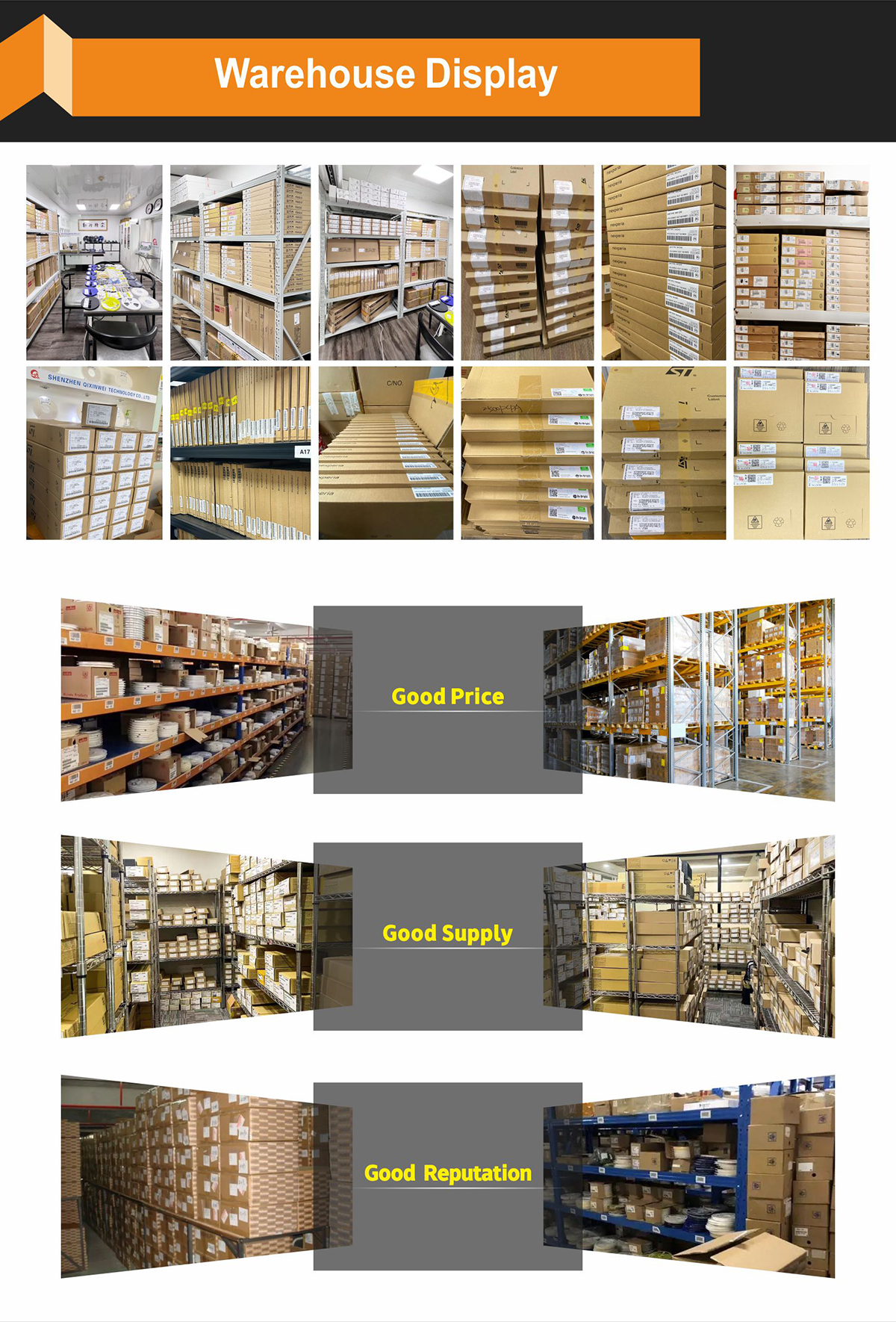
Massive In-Stock Inventory – Ready to ship promptly
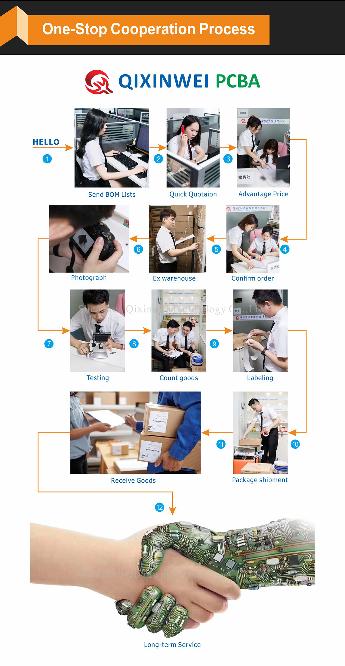
BOM Matching Service – One-stop solution, save time
PCBA Customization – Professional engineering team creates tailor-made solutions based on your needs
Cost-Effective & Efficient – Better channel, better cost
A dedicated team makes your procurement smoother.
Contact us for BOM quotes or PCBA inquiries

FAQ
1. What is the STM32F103ZET6 Development Board / Core Board?
The STM32F103ZET6 Development Board / Core Board is an embedded learning and development platform based on the STM32F103ZET6 MCU, featuring an ARM® Cortex®-M3 32-bit RISC core. The core board integrates essential circuits for MCU operation including crystal oscillator and USB control circuitry, with all I/O resources accessible. The development board adds richer on-board peripherals and interfaces for various experiments and project development.
2. What are the key specifications of the STM32F103ZET6 Development Board / Core Board?
MCU: STM32F103ZET6, ARM Cortex-M3 32-bit RISC core
Frequency: 72MHz, 1.25 DMIPS/MHz
Memory: 512KB Flash, 64KB SRAM
Package: LQFP144
Operating Voltage: 2V ~ 3.6V
I/O Count: 112
3. What package does the STM32F103ZET6 use?
The MCU uses an LQFP144 package. Core boards typically use 2.0mm pitch pin headers to expose all I/Os in a compact form factor suitable for embedded systems; development boards feature richer interface layouts for peripheral expansion.
4. What applications is the STM32F103ZET6 Development Board / Core Board suitable for?
It is widely used in industrial control, medical devices, Human-Machine Interfaces (HMI) , IoT nodes, motor drives, data acquisition and signal processing, and embedded system learning. The STM32F103ZET6 is the highest-end configuration in the STM32F1 series, particularly suited for complex applications requiring large storage and rich peripherals.
5. What development tools support the STM32F103ZET6 Development Board / Core Board?
Recommended tools include Keil MDK-ARM (with STM32F1 Device Family Pack installed) and STM32CubeIDE. STM32CubeMX can be used for peripheral initialization code generation and clock tree configuration. Open-source solutions like VSCode + PlatformIO are also well-supported.
6. What is the operating temperature range of the STM32F103ZET6 Development Board / Core Board?
The chip's operating temperature range is -40°C to +85°C (ambient temperature).
7. What debug and programming interfaces does the STM32F103ZET6 support?
It supports both JTAG and SWD (Serial Wire Debug) interfaces. Some development boards also feature a one-click download function, allowing program programming via a single USB cable without the need to frequently adjust BOOT jumpers.
8. What peripheral interfaces does the STM32F103ZET6 support?
Communication: 5×USART, 3×SPI, 2×I2C, 2×I2S, 1×CAN, 1×USB
Memory Expansion: 1×FSMC (supports NOR/NAND/SRAM expansion)
Memory Card: 1×SDIO
Analog: 3×12-bit ADC (21 channels), 2×12-bit DAC
Timers: 2 basic timers, 4 general-purpose timers, 2 advanced timers
DMA: 2 DMA controllers with 12 channels total
9. What is the difference between STM32F103ZET6 and STM32F103VET6?
In the naming convention, Z indicates 144 pins and E indicates 512KB Flash. The STM32F103VET6 uses an LQFP100 package (100 pins), while the STM32F103ZET6 uses an LQFP144 package (144 pins) with more I/Os (112) and stronger peripheral expansion capabilities. The STM32F103ZET6 is positioned for high-performance applications, suitable for complex systems such as industrial control and medical devices.
10. What power supply options does the STM32F103ZET6 Development Board / Core Board support?
Multiple power supply options are supported: USB power (via Micro USB/Type-C interface), 5V DC input (via power jack or 5Vin pin), and JTAG/SWD debugger power. An on-board AMS1117-3.3 LDO regulator converts input voltage to 3.3V for the MCU. Some development boards also feature a VBAT backup battery holder (supporting CR1220 coin cell batteries) for RTC clock retention.


