
qixinwei-pcba


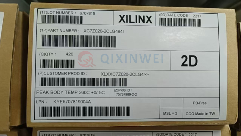
XC7Z020-2CLG484I Xilinx Zynq-7000 Dual-Core ARM Cortex-A9 + Artix-7 FPGA SoC Processor Chip FBGA484 Package
XC7Z020-2CLG484I Product Overview
The XC7Z020-2CLG484I is a Zynq-7000 All Programmable SoC from Xilinx, innovatively integrating a dual-core ARM Cortex-A9 MPCore processor with Artix™-7 FPGA programmable logic on a single chip. Manufactured on a 28nm HKMG process, XC7Z020-2CLG484I operates at up to 766MHz with a core voltage of 1.0V, in a 484-CSPBGA (19x19mm) package. The PS features 256KB on-chip RAM, while the PL provides 85K logic cells, 220 DSP Slices, and 4.9Mb Block RAM. Supporting an industrial temperature range of -40℃ to +100℃, XC7Z020-2CLG484I heterogeneous SoC combines software programmability with hardware customizability and is widely used in industrial automation, communications, machine vision, automotive electronics, medical devices, and edge computing.
XC7Z020-2CLG484I Key Features
XC7Z020-2CLG484I Heterogeneous Computing Architecture (PS + PL): The core advantage of the XC7Z020-2CLG484I lies in its unique SoC architecture, achieving seamless collaboration between the Processing System (PS) and Programmable Logic (PL). The PS and PL are interconnected via a high-speed AXI bus. Users can implement hardware acceleration (e.g., signal filtering, image preprocessing) via the FPGA while the ARM processor runs a real-time operating system (RTOS) for complex control logic.
XC7Z020-2CLG484I Processing System (PS) – Dual-Core ARM Cortex-A9: Features a dual-core ARM Cortex-A9 MPCore processor based on the ARMv7-A architecture, operating at up to 767MHz. Each core delivers 2.5 DMIPS/MHz. Integrated NEON media processing engine and Floating-Point Unit (FPU) . Cache system features 2×32KB L1 I/D cache + 512KB L2 shared cache, with 256KB on-chip RAM.
XC7Z020-2CLG484I Programmable Logic (PL) – Artix-7 FPGA: Based on the 28nm Artix-7 FPGA architecture, providing 85K logic cells (equivalent to 53.2K lookup tables), 220 DSP Slices, and 4.9Mb Block RAM. Features 106,400 flip-flops, 48 LVDS differential pairs, and 100 voltage-adjustable IOs. Total PL I/Os reach 198.
XC7Z020-2CLG484I Rich Memory and Interfaces: Supports DDR3/DDR3L/DDR2/LPDDR2 memory types with 32-bit bus, data rates up to 1066Mbps, expandable to 1GB. Compatible with QSPI Flash (up to 256MBit) and eMMC Flash (up to 8GB).
XC7Z020-2CLG484I Comprehensive Peripheral Interfaces: Features 2×Gigabit Ethernet (with IEEE 1588), 2×USB 2.0 OTG, 2×CAN 2.0B, and multiple SPI/I2C/UART interfaces. I/O voltage supports 1.8V~3.3V range.
XC7Z020-2CLG484I Industrial-Grade Temperature & Security: Operating temperature range -40℃ to +100℃ (TJ) . Built-in RSA authentication, AES, and SHA 256-bit encryption. Integrated 2×1MSPS AD converters for on-chip voltage and temperature monitoring.
XC7Z020-2CLG484I Applications
The XC7Z020-2CLG484I is widely used in:
Industrial Automation & Control: Motor control, PLCs, sensor fusion, industrial robotics
Communications: 5G small cell signal processing
Machine Vision & Embedded Vision: Industrial machine vision
Automotive: Multi-camera driver assistance systems (ADAS)
Medical Devices: Medical endoscopes
Edge Computing & AIoT: AR/VR video processing, drone flight control
Consumer Electronics: 4K2K UHD TV
Why Choose QIXINWEI
Years of experience in the electronics industry. Trusted by global customers.
Massive In-Stock Inventory – Ready to ship promptly
BOM Matching Service – One-stop solution, save time
PCBA Customization – Professional engineering team creates tailor-made solutions based on your needs
Cost-Effective & Efficient – Better channel, better cost
A dedicated team makes your procurement smoother.
Contact us for BOM quotes or PCBA inquiries






FAQ:
1 What is the XC7Z020-2CLG484I chip
XC7Z020-2CLG484I is a Zynq 7000 System on Chip from Xilinx that integrates a dual core ARM Cortex A9 processor with Artix 7 FPGA programmable logic on a single die.
2 What are the processing system and FPGA logic resources
XC7Z020-2CLG484I has a Processing System that includes a dual core ARM Cortex A9 processor running at up to 766 megahertz. The Programmable Logic offers approximately 85 thousand logic cells along with DSP slices and block RAM.
3 What package pin count and physical size does XC7Z020-2CLG484I use
XC7Z020-2CLG484I uses a CLG484 BGA ball grid array package with 484 pins featuring a fine pitch and high density IO resources suitable for high performance highly integrated PCB designs.
4 What are the temperature grade and speed grade
The XC7Z020-2CLG484I suffix I denotes industrial grade with an operating temperature range from minus 40 degrees Celsius to plus 100 degrees Celsius. The 2 indicates the speed grade ensuring high performance and processing throughput.
5 What application scenarios is XC7Z020-2CLG484I chip suitable for
XC7Z020-2CLG484I is widely used in industrial automation control machine vision image processing high end communication equipment medical imaging instruments and edge AI acceleration computing.
6 What peripheral interfaces does XC7Z020-2CLG484I support
XC7Z020-2CLG484I supports Gigabit Ethernet USB 2.0 and 3.0 SD card controllers SPI I2C UART and abundant general purpose IO pins to meet diverse communication and expansion needs.
7 What type of external memory does XC7Z020-2CLG484I support
XC7Z020-2CLG484I features a built in DDR memory controller supporting high speed SDRAM such as DDR3 and DDR3L with typical configurations providing 1GB to 2GB of memory capacity.
8 What are the development environment and tools
Hardware development uses the official Xilinx Vivado design suite for logic design while embedded ARM software development uses the Vitis platform or SDK supporting C and C plus plus languages.
9 What are the PCB design requirements for the BGA package
Due to the extremely dense pin array PCB designs require high layer count boards using blind or buried vias for fan out and strict impedance and length matching for high speed differential signals.
10 How is the power supply voltage divided and what precautions are needed
XC7Z020-2CLG484I requires multiple independent power rails including core voltages IO voltages auxiliary voltages and DDR reference voltages on both the PS and PL sides. The design must strictly follow the official Xilinx power on sequencing requirements.
- Model Number:
- XC7Z020-2CLG484I
- Brand:
- Xilinx
- Product Series:
- Zynq-7000
- Architecture:
- MCU + FPGA
- CPU Speed:
- 766MHz
- Performance per Core:
- 2.5 DMIPS/MHz
- FPGA Logic Cells:
- 85K
- Block RAM:
- 4.9Mb(630KB)
- Operating Temperature:
- -40℃ ~ +100℃
- Operating Voltage:
- 1.8V~3.3V


