
qixinwei-pcba


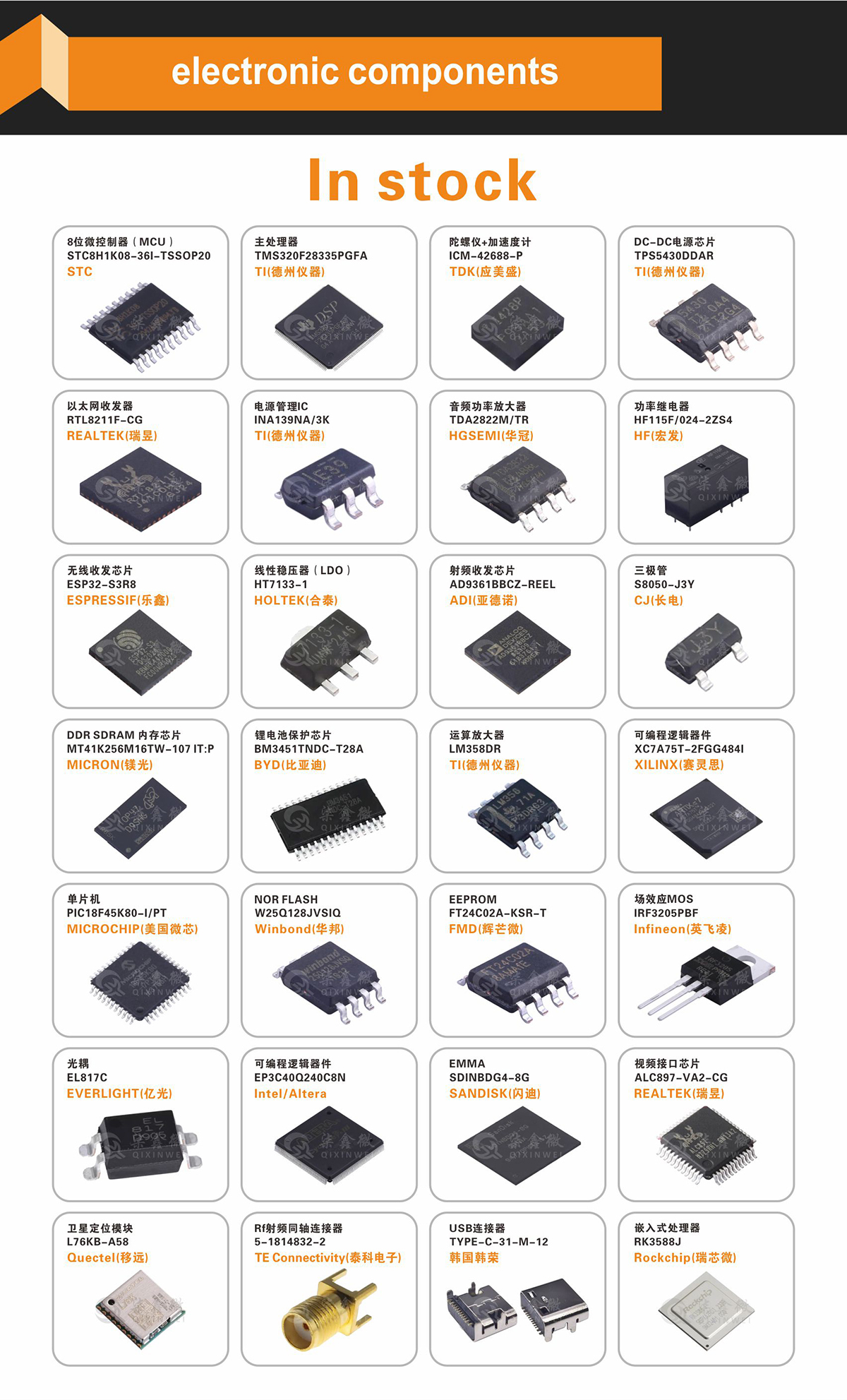
STM32H743IIK6 ST Mainstream Arm Cortex-M7 High-Performance 32-bit MCU 2MB Flash 1MB SRAM LCD-TFT Chrom-ART JPEG CAN FD USB OTG Ethernet Crypto UFBGA-176+25
STM32H743IIK6 Product Overview
STM32H743IIK6 is a Cortex-M7 MCU at 480 MHz with double-precision FPU, UFBGA-176+25. 2 MB dual-bank Flash, 1 MB SRAM, LCD-TFT controller (up to XGA), Chrom-ART accelerator (DMA2D), hardware JPEG codec, Ethernet MAC, USB OTG HS/FS (HS requires external ULPI PHY), CAN FD, HW crypto (AES/CRYP/HASH/RNG), dual Quad SPI, FMC (SDRAM), three 16-bit ADCs (5 Msps, 24 ch), two 12-bit DACs, two comparators, two op-amps, advanced motor control timers, GP/LP timers, RTC, 8×USART/UART, 5×SPI/I2S, 4×I2C, SDIO, SAI, SPDIF-Rx. Up to 168 x 5 V-tolerant I/Os. 1.62–3.6 V, -40–85 °C. Compared to the LQFP-208 H743BIT6, this model uses an ultra-compact UFBGA-176+25 package, drastically reducing PCB footprint while retaining the same powerful graphics, real-time control, and secure networking capabilities — ideal for space-constrained high-end embedded applications.
STM32H743IIK6 Core Features
Core: Cortex-M7 480 MHz, DPFPU + L1 cache (16 KB I-cache + 16 KB D-cache)
Memory: 2 MB Dual-Bank Flash, 1 MB SRAM (incl. large DTCM and ITCM)
Graphics & Multimedia: LCD-TFT controller (up to XGA), Chrom-ART accelerator (DMA2D), HW JPEG codec
Connectivity: Ethernet MAC, USB OTG HS/FS (HS needs external ULPI PHY), CAN FD, SDIO, SAI, SPDIF-Rx, 8×USART/UART, 5×SPI/I2S, 4×I2C
Security: Hardware AES/CRYP/HASH/RNG crypto coprocessor
Analog: 3×16-bit ADCs (5 Msps, 24 ch), 2×12-bit DACs, 2×Comparators, 2×Op-Amps
Motor Control: 2×Advanced Timers (PWM/Deadtime/Brake), multiple GP/LP timers
Memory Expansion: FMC (SDRAM/PSRAM/NOR/NAND), Dual Quad SPI
I/Os: 168 (5 V-tolerant)
Package: UFBGA-176+25
Temperature Range: -40°C to 85°C
STM32H743IIK6 Applications
Advanced HMI: Industrial touchscreens, graphical dashboards, smart home control panels
Real-Time Control & Networking: High-end PLCs, servo drives, industrial Ethernet gateways
Security Systems: Secure communication nodes, data encryption terminals
Multimedia Processing: JPEG image compression/decompression, digital audio equipment
Space-Constrained Devices: High-performance handheld devices, portable medical instruments, precision data acquisition
STM32H743IIK6 Key Advantages
480 MHz Cortex-M7 + DPFPU: Ultimate real-time processing and floating-point performance
2 MB Flash + 1 MB SRAM: Massive storage for complex code and large data buffers
LCD-TFT + Chrom-ART + JPEG: Full hardware graphics and image acceleration for smooth displays and fast image processing
Ethernet + CAN FD + HW Crypto: Single-chip for industrial networking, real-time communication, and data security
Ultra-Compact UFBGA-176+25 Package: 168 I/Os in a minimal footprint, saving PCB space
Dual Quad SPI + FMC: Flexible external memory expansion
1.62–3.6 V Wide Supply: Adaptable to various power scenarios
Why Choose QIXINWEI
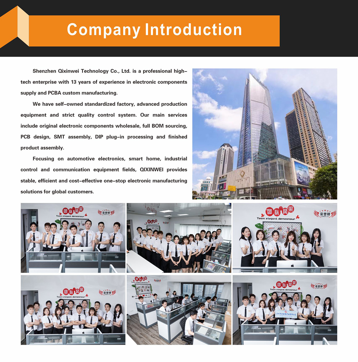
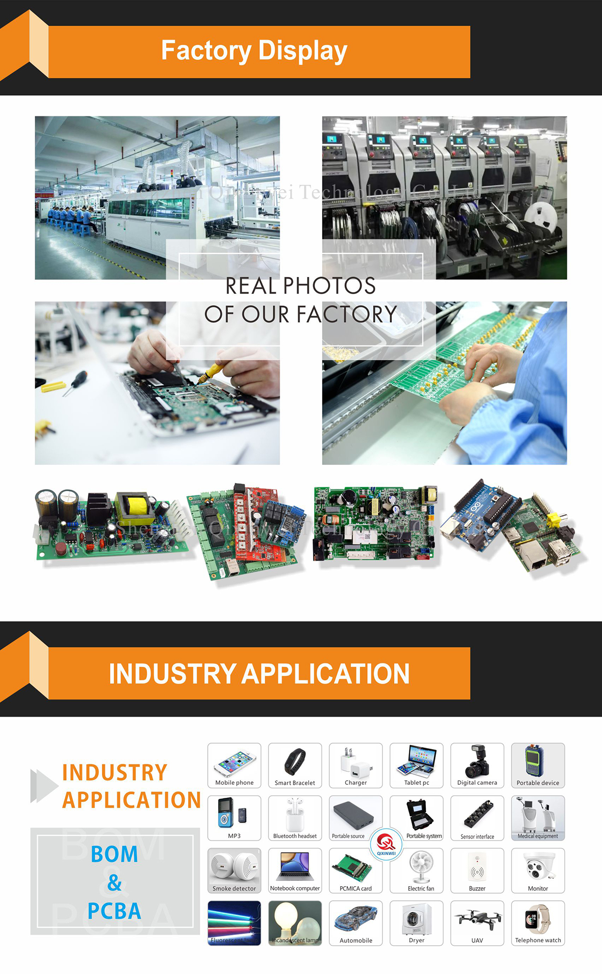
Years of experience in the electronics industry. Trusted by global customers.
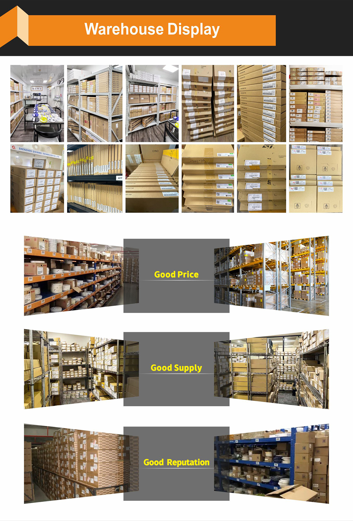
Massive In-Stock Inventory – Ready to ship promptly.
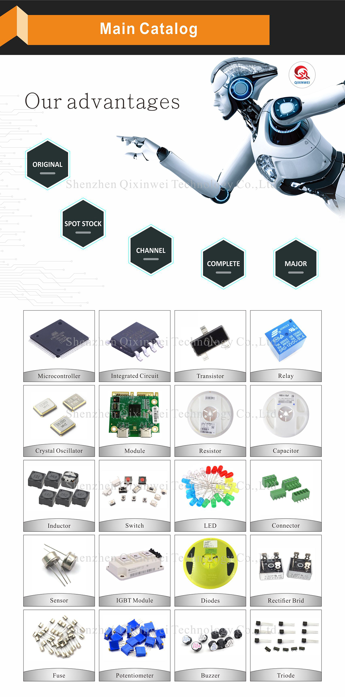
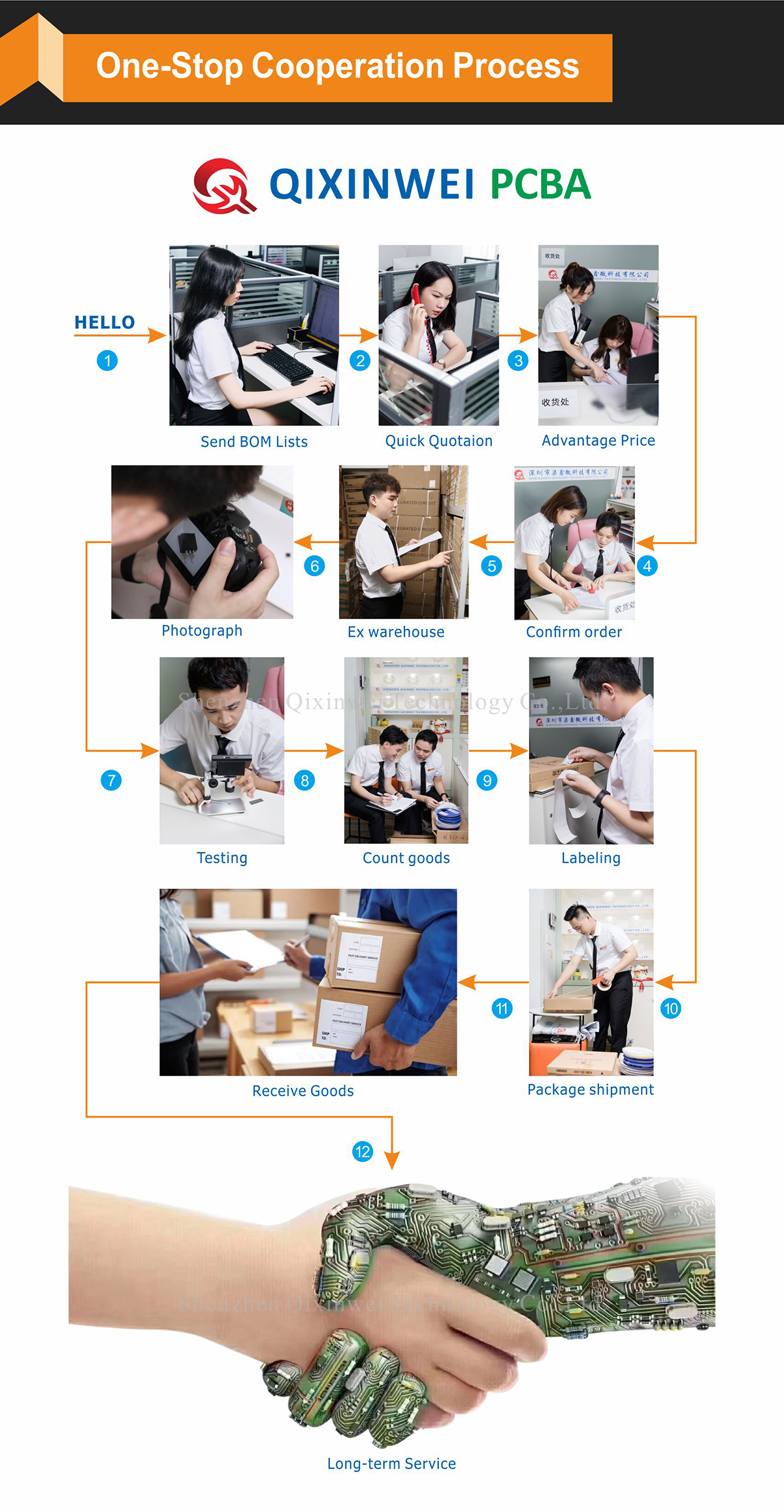
BOM Matching Service – One-stop solution, save time.
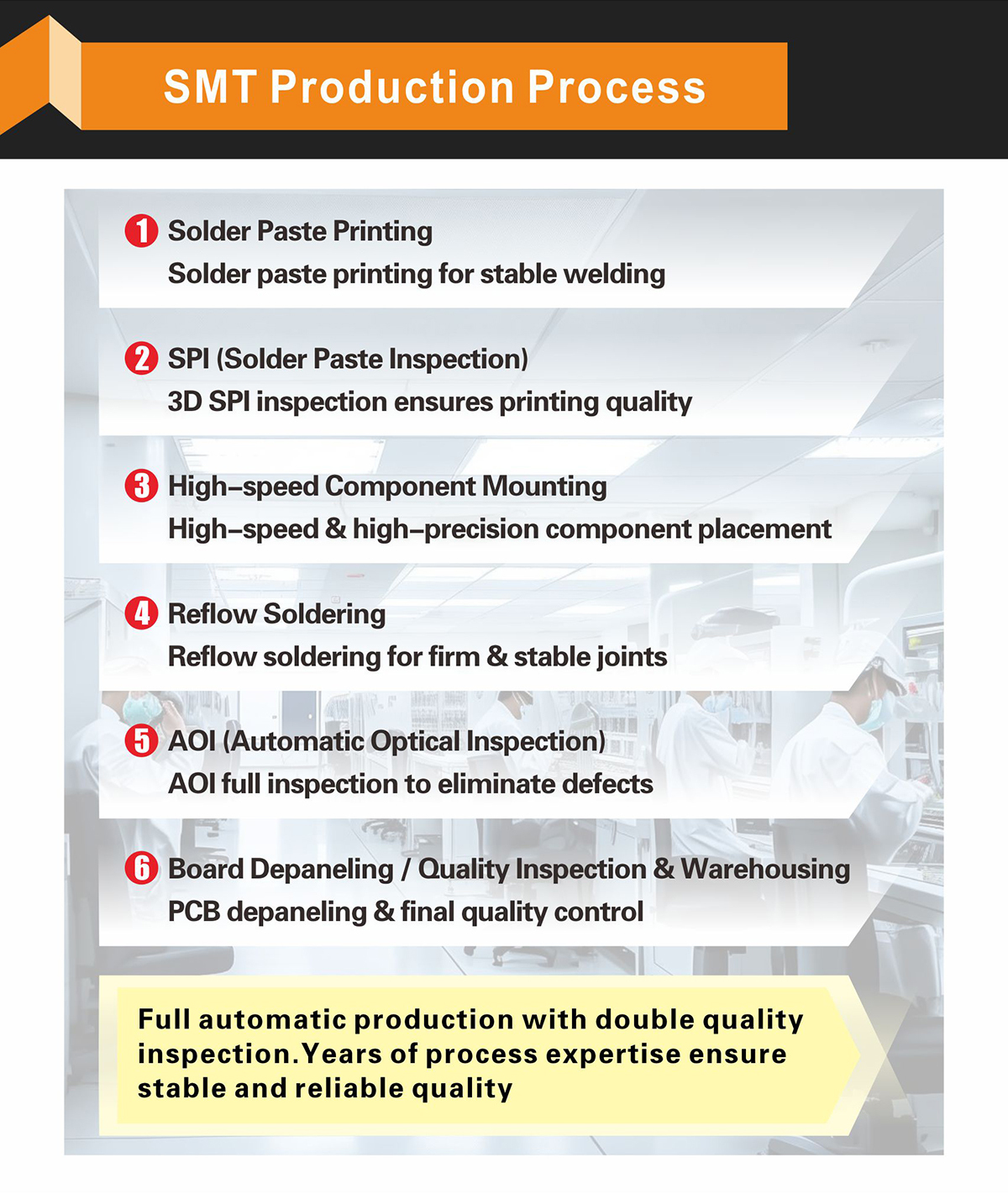
PCBA Customization – Professional engineering team creates tailor-made solutions based on your needs.
Cost-Effective & Efficient – Better channel, better cost.
A dedicated team makes your procurement smoother.
Contact us for BOM quotes or PCBA inquiries.


FAQ
1. What package does the STM32H743IIK6 use, and what advantages does it have over the LQFP‑packaged STM32H743IIT6?
The STM32H743IIK6 comes in a UFBGA‑176 package (0.65 mm ball pitch, 10 mm × 10 mm) providing up to 140 usable I/Os, whereas the LQFP‑176 IIT6 measures 24 mm × 24 mm. The BGA package delivers the same peripheral breakout capability in a much smaller PCB area, making it ideal for space‑constrained yet interface‑rich compact devices. However, BGA requires reflow soldering and is not hand‑solderable, so it is better suited for volume SMT production. If hand‑solderability and visual inspection are priorities, the IIT6’s LQFP package is more friendly.
2. How difficult is it to solder the UFBGA‑176 package (0.65 mm pitch)? Is low‑volume production feasible?
The 0.65 mm pitch is moderate by BGA standards, but reflow soldering or a professional BGA rework station is still required—hand soldering with an iron is not possible. For low‑volume production, good yields can be achieved with proper stencil design and controlled reflow profiles. It is strongly recommended to develop and debug on a NUCLEO‑H743ZI or Discovery board during prototyping, and only transition to the BGA for volume production after the hardware design is finalized.
3. How is the 2 MB dual‑bank Flash used in practice? How can safe OTA updates be implemented?
Dual‑bank Flash allows the CPU to execute current firmware from one bank while erasing and writing new firmware to the other. During an update, the new firmware is downloaded to the alternate bank and verified; a simple boot‑address switch then completes the upgrade. If a power loss or verification failure occurs, the system automatically rolls back to the original firmware, guaranteeing the device always remains operational. This mechanism is critical for industrial gateways, medical equipment, and infrastructure nodes requiring 24/7 uptime.
4. How is the 1 MB SRAM organized, and how does the multi‑bank architecture benefit real‑time control?
The 1 MB SRAM is partitioned into DTCM (Data Tightly Coupled Memory), ITCM (Instruction Tightly Coupled Memory), AXI SRAM, and multiple AHB SRAM blocks. DTCM and ITCM provide zero‑wait‑state CPU access for the lowest and most deterministic interrupt and control‑loop latency. The multi‑bank design allows DMA and the CPU to access different memory regions simultaneously without blocking, significantly improving data throughput when concurrently handling Ethernet, LCD refresh, high‑speed ADC acquisition, and motor control.
5. Can the Chrom‑ART accelerator and LCD controller be fully utilized in the UFBGA‑176 package? What display size can be driven?
Yes, fully. The Chrom‑ART (DMA2D) hardware accelerator does not consume extra I/Os, so its functionality is package‑independent. The on‑chip TFT‑LCD controller (LTDC) has ample pins among the 140 I/Os to bring out a full 24‑bit RGB interface, directly driving displays up to 1024×768 with smooth TouchGFX UIs. Compared to packages with fewer I/Os, the IIK6 offers more relaxed pin allocation between graphics and other peripherals.
6. What hardware security modules are integrated? Does it support secure boot and firmware encryption?
It integrates a hardware true‑random‑number generator (TRNG), AES‑256, SHA‑1/SHA‑2, and HMAC accelerators for efficient encryption and hashing. Combined with dual‑bank Flash and code readout protection (RDP), it can implement a complete chain of trust from secure boot to encrypted firmware updates. This is especially important in payment terminals, secure gateways, and industrial controllers where firmware IP must be protected from unauthorized access, tampering, or cloning.
7. How much external memory can be simultaneously connected via FMC and dual QSPI? Can both 32‑bit SDRAM and dual QSPI Flash coexist?
Absolutely. The Flexible Memory Controller (FMC) supports 32‑bit SDRAM, up to 256 MB of runtime memory, and can also interface with parallel NOR/NAND Flash. The dual Quad SPI interfaces support memory‑mapped mode and can connect high‑speed NOR Flash or HyperRAM. These interfaces do not conflict; with the UFBGA‑176’s generous pin count, you can simultaneously use 32‑bit SDRAM for data buffering, dual QSPI Flash for code and assets, and still have room for multiple SDMMC and other peripherals—creating a highly flexible memory architecture.
8. In the 176‑pin package, can Ethernet, USB HS, multiple CAN FD channels, and SDMMC be used concurrently without pin conflicts?
Thanks to the 140 available I/Os, Ethernet RMII (~9 pins), USB HS ULPI (~12 pins), two FDCAN channels (4 pins), and SDMMC (~6 pins) can all be brought out simultaneously, with plenty of GPIOs remaining for UARTs, SPIs, I²Cs, and more. Compared to packages with fewer I/Os, the IIK6 greatly reduces pin‑conflict headaches, making it an ideal core for industrial gateways, vehicle communication modules, and distributed controllers.
9. How should power and thermal management be handled at 480 MHz full load? Any recommendations for the BGA thermal pad design?
Typical power consumption at full load is around 1–1.5 W. The UFBGA‑176 package does not have an exposed thermal pad; heat is primarily conducted through internal GND balls and the PCB ground planes. It is recommended to use as much continuous ground copper as possible on all PCB layers beneath the chip, and to add multiple thermal vias connecting the ground layers to enhance heat dissipation. Within the commercial temperature range (0 °C–85 °C), good PCB thermal design ensures stable long‑term operation.
10. Is the software toolchain for the STM32H743IIK6 mature? Can I reuse code from previous STM32F4/F7 projects?
Very mature. It is fully compatible with the STM32Cube ecosystem, including free tools such as STM32CubeMX and STM32CubeIDE, and the feature‑rich STM32CubeH7 firmware package. If you have previously developed on STM32F4 or F7, a large portion of HAL code can be reused, with the main adjustments being peripheral configuration and memory mapping. ST also provides extensive example projects covering Ethernet, USB, graphics, and file systems to help jump‑start development.
- Property:
- Specification
- Product Type:
- Arm Cortex-M7 High-Performance 32-bit MCU
- Brand:
- STMicroelectronics
- Core:
- Cortex-M7 480 MHz (Double-Precision FPU)
- Package:
- UFBGA-176+25
- Memory:
- 2 MB Flash, 1 MB SRAM
- Graphics & Multimedia:
- LCD-TFT, Chrom-ART, HW JPEG
- Connectivity:
- Ethernet, USB OTG HS/FS, CAN FD
- Security:
- AES/CRYP/HASH/RNG
- Analog:
- 3×16-bit ADCs, 2×12-bit DACs, 2×Op-Amps, 2×Comparators
- I/Os:
- 168
- Voltage:
- 1.62V–3.6V
- Temperature:
- -40°C to 85°C


