
qixinwei-pcba


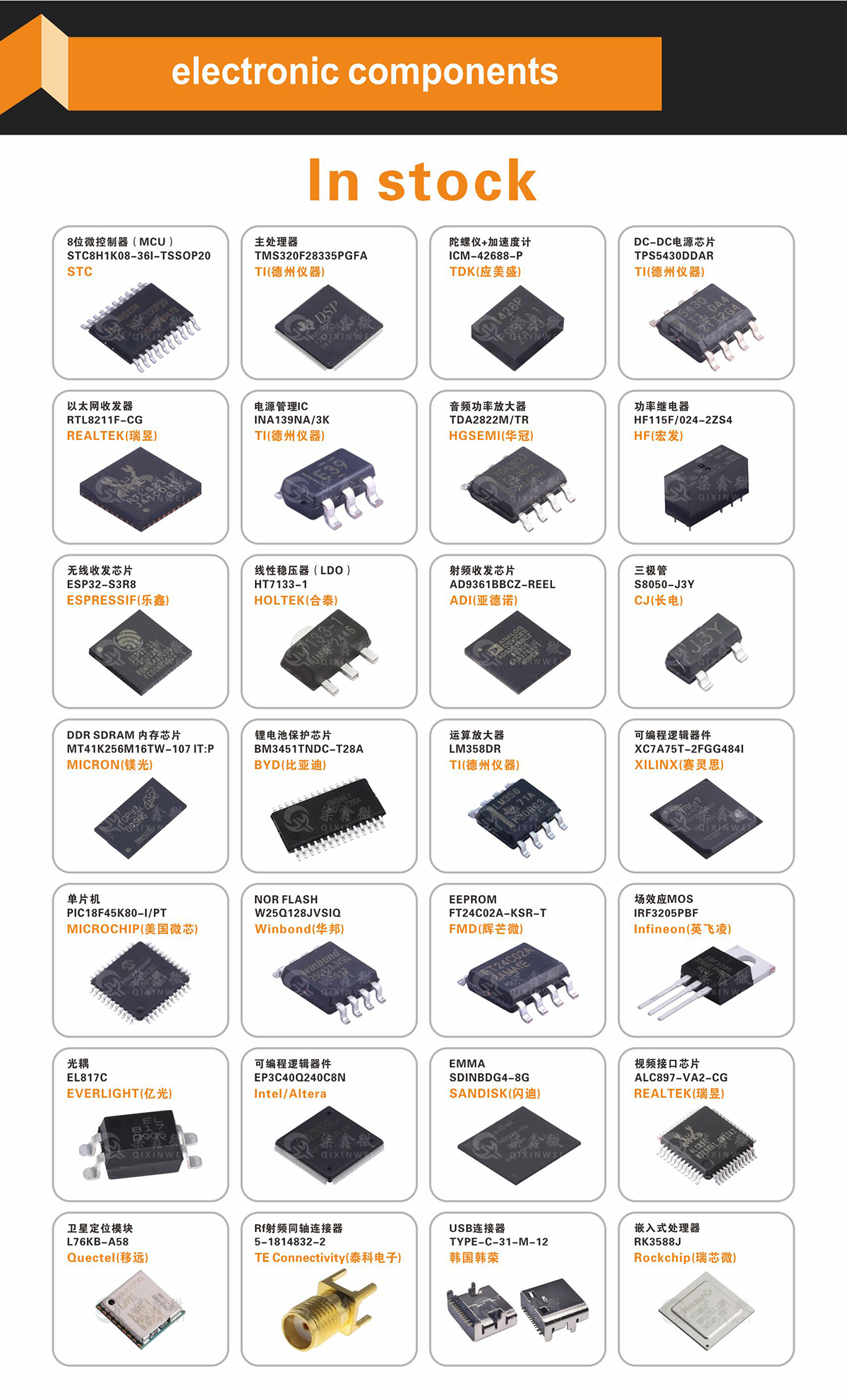
STM32H723ZGT6 ST Mainstream Arm Cortex-M7 High-Performance 32-bit MCU 1MB Flash 564KB SRAM CAN FD USB OTG Ethernet LQFP-144
STM32H723ZGT6 Product Overview
STM32H723ZGT6 is a Cortex-M7 MCU at 550 MHz with double-precision FPU, LQFP-144. 1 MB dual-bank Flash, 564 KB SRAM, USB OTG HS/FS (on-chip HS PHY), Ethernet MAC, CAN FD, dual Quad SPI, FMC (SDRAM), three 16-bit ADCs (5 Msps, 24 ch), two 12-bit DACs, two comparators, two op-amps, advanced motor control timers, GP/LP timers, RTC, 8×USART/UART, 5×SPI/I2S, 4×I2C, SDIO, SAI, SPDIF-Rx. 114 x 5 V-tolerant I/Os. 1.71–3.6 V, -40–85 °C. Compared to the STM32H723ZET6 (512 KB Flash), this model doubles the Flash to 1 MB, providing ample code space for complex real-time control and industrial networking — the top-tier 144-pin model in the H723 series.
STM32H723ZGT6 Core Features
Core: Cortex-M7 550 MHz, DPFPU + L1 cache (16 KB I-cache + 16 KB D-cache)
Memory: 1 MB Dual-Bank Flash, 564 KB SRAM (incl. 128 KB DTCM)
Connectivity: Ethernet MAC, USB OTG HS/FS (on-chip HS PHY), CAN FD, SDIO, SAI, SPDIF-Rx, 8×USART/UART, 5×SPI/I2S, 4×I2C
Analog: 3×16-bit ADCs (5 Msps, 24 ch), 2×12-bit DACs, 2×Comparators, 2×Op-Amps
Motor Control: 2×Advanced Timers (PWM/Deadtime/Brake), multiple GP/LP timers
Memory Expansion: FMC (SDRAM/PSRAM/NOR/NAND), Dual Quad SPI
I/Os: 114 (5 V-tolerant)
Package: LQFP-144
Temperature Range: -40°C to 85°C
STM32H723ZGT6 Applications
Industrial Control: Real-time controllers, PLCs, servo drives, industrial Ethernet gateways
High-Speed Communication: Ethernet/CAN FD/USB HS interface conversion and bridging
Audio & Consumer: Digital audio equipment, advanced consumer electronics
Motor Control: High-precision FOC, multi-axis servo control
Portable Medical & Instrumentation: High-performance handheld devices, precision data acquisition
STM32H723ZGT6 Key Advantages
550 MHz Cortex-M7 + DPFPU: Ultimate real-time processing and floating-point performance
1 MB Dual-Bank Flash: Large storage for safe firmware updates and complex applications
On-Chip USB HS PHY: Eliminates external HS PHY, simplifying design and BOM
Ethernet + CAN FD + Rich Connectivity: Single-chip for industrial networking and real-time communication
114 I/Os + 24 ADC Channels: Rich pin and analog acquisition resources for complex system integration
Dual Quad SPI + FMC: Flexible external memory expansion
1.71–3.6 V Wide Supply: Adaptable to various power scenarios
Why Choose QIXINWEI
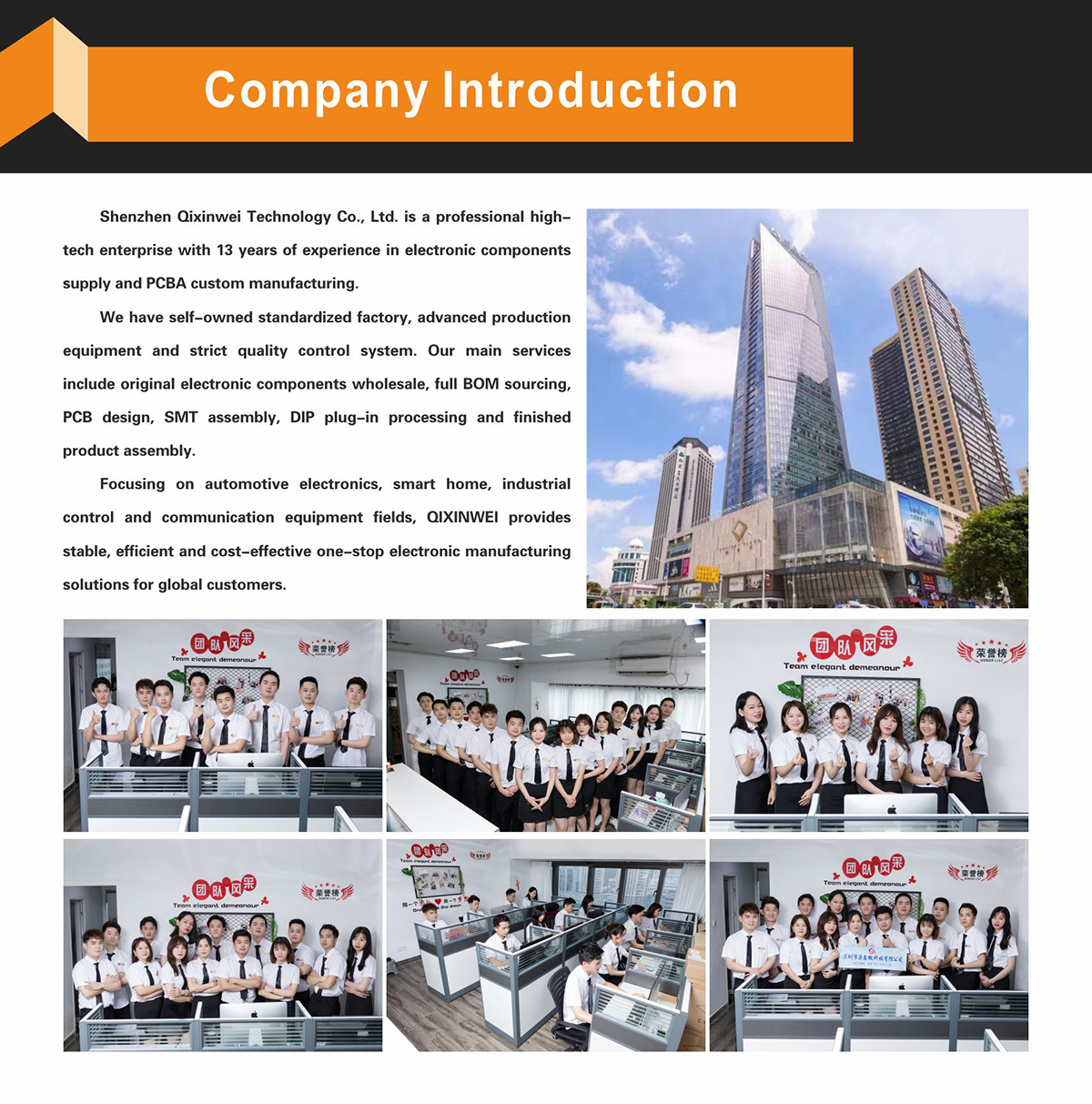
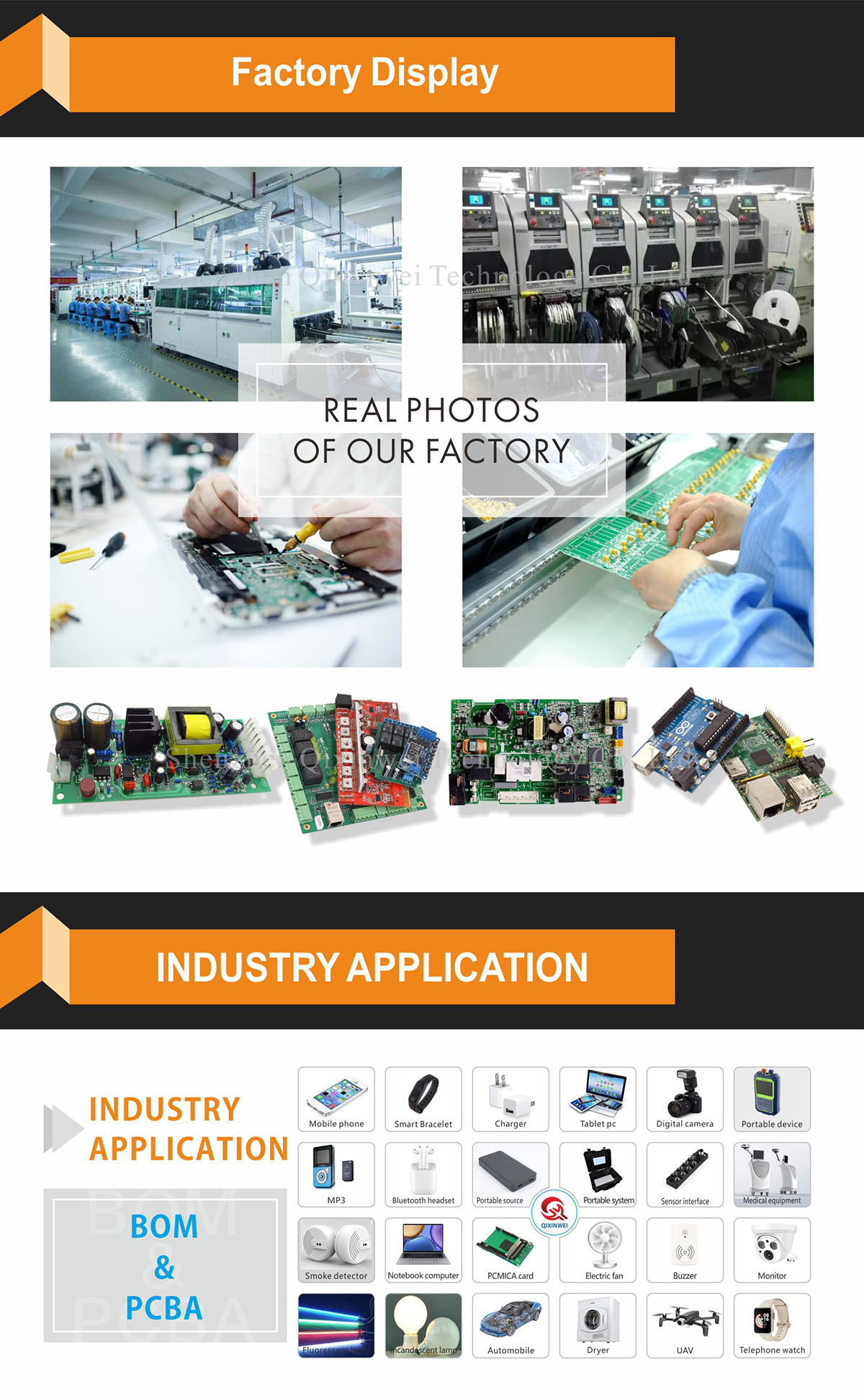
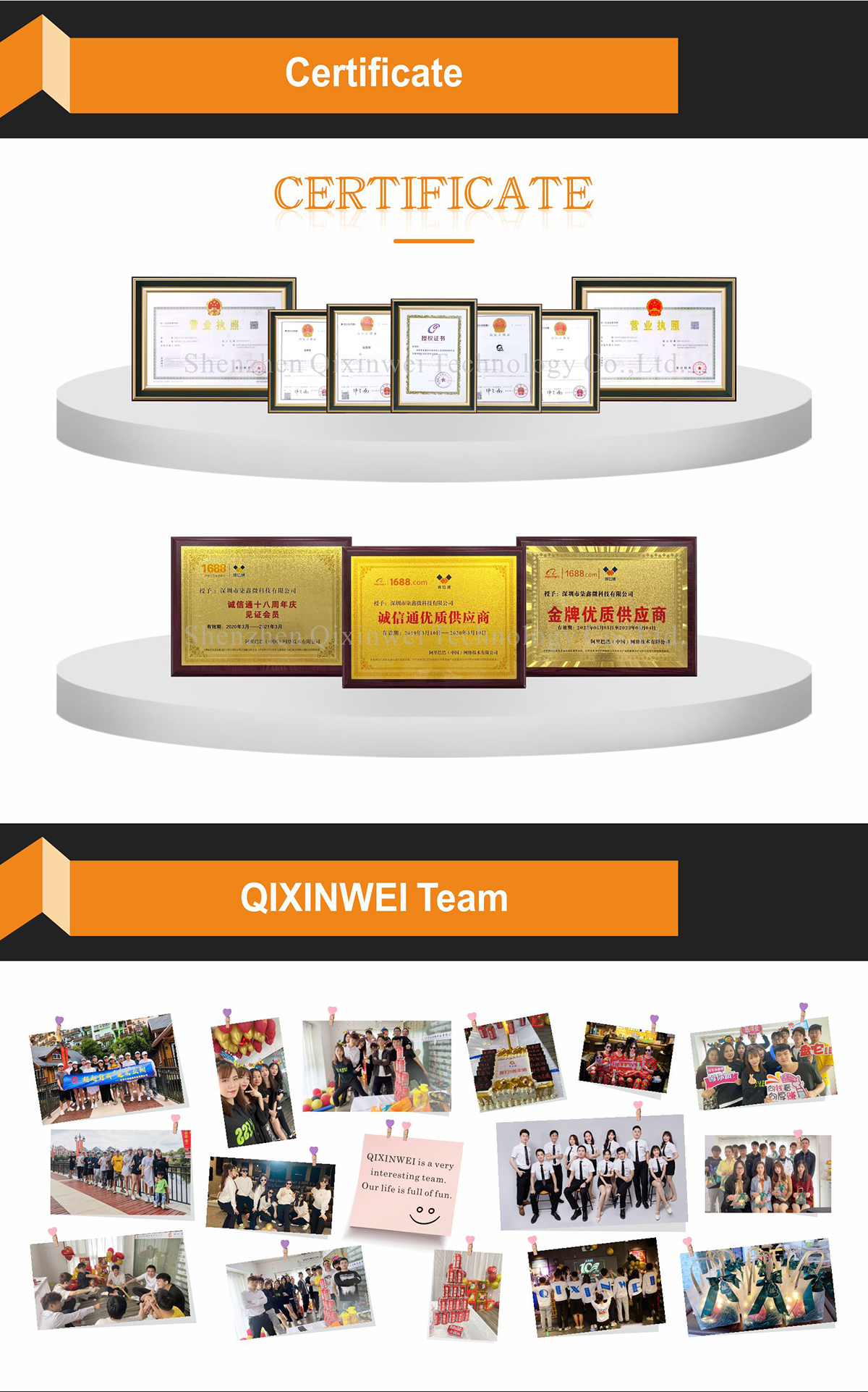
Years of experience in the electronics industry. Trusted by global customers.
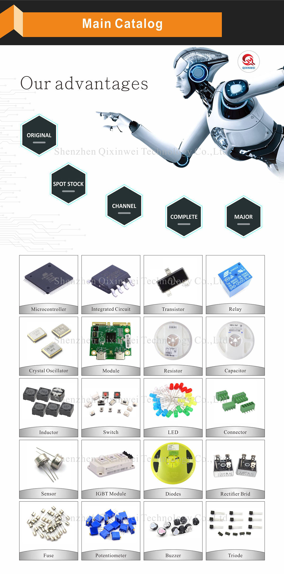
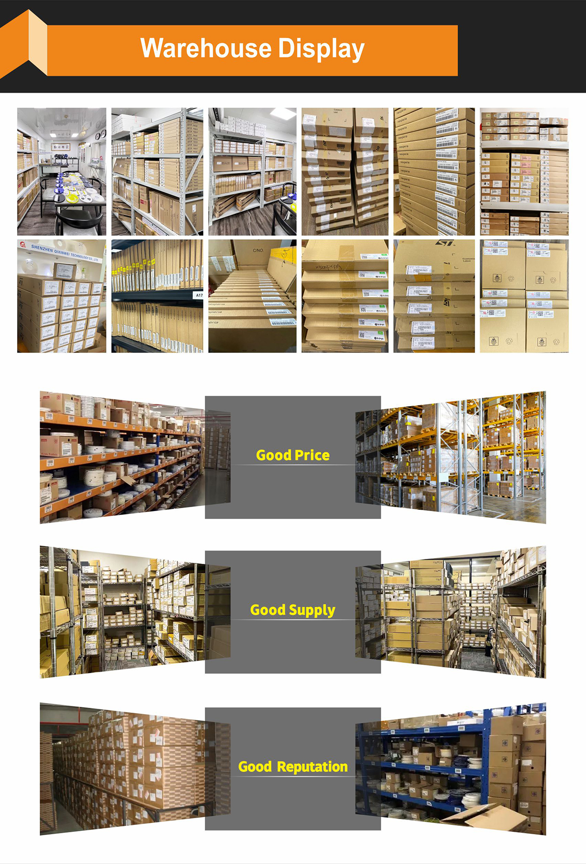
Massive In-Stock Inventory – Ready to ship promptly.
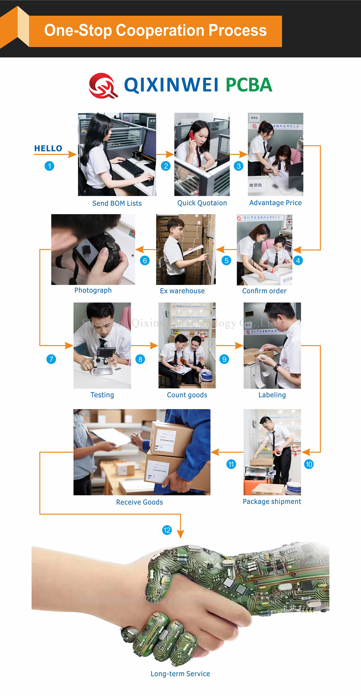
BOM Matching Service – One-stop solution, save time.
PCBA Customization – Professional engineering team creates tailor-made solutions based on your needs.
Cost-Effective & Efficient – Better channel, better cost.
A dedicated team makes your procurement smoother.
Contact us for BOM quotes or PCBA inquiries.


FAQ
1. The Cortex‑M7 core on the STM32H723ZGT6 runs at up to 550 MHz. What advantages does this offer over the 480 MHz STM32H743?
The 550 MHz Cortex‑M7 delivers approximately 1178 DMIPS and 2778 CoreMark—a roughly 15% performance uplift over the 480 MHz H743. With the same double‑precision FPU, DSP extensions, 1 MB dual‑bank Flash, 564 KB SRAM, and a complete hardware crypto accelerator in an LQFP‑144 package, it is particularly well‑suited for industrial control, motor drives, and communication gateways that demand rigorous real‑time computation, data security, and cost efficiency.
2. How does the STM32H723ZGT6 differ from the STM32H725ZGT6? Which one should I choose?
Both are extremely similar in core, memory, and most peripherals. However, the H723 series usually integrates a more comprehensive hardware security suite—including AES‑256, SHA‑1/SHA‑2, and HMAC accelerators—while the H725 may omit or simplify some of these security features to reduce cost. If your system requires firmware encryption, secure boot, or secure communication (e.g., IoT gateways, payment terminals), the H723 is the better fit; if those security functions are not essential, the H725 can deliver nearly identical real‑time processing at a lower price point.
3. How is the 564 KB SRAM organized, and how does it benefit hard real‑time tasks?
The SRAM is carefully partitioned into 128 KB DTCM (Data Tightly Coupled Memory), 64 KB ITCM (Instruction Tightly Coupled Memory), 256 KB AXI SRAM, and 128 KB low‑power SRAM (retainable in Stop mode). DTCM and ITCM provide zero‑wait‑state CPU access for the lowest and most deterministic interrupt and control‑loop latency. The multi‑bank architecture allows DMA and the CPU to access different regions simultaneously without blocking, significantly boosting throughput when concurrently handling Ethernet, LCD refresh, and high‑speed ADC acquisition.
4. Does the 1 MB dual‑bank Flash support OTA updates? How can update safety be ensured?
Fully supported. The dual‑bank architecture allows code execution from one bank while the other is being erased and programmed. Once a new firmware image is downloaded to the alternate bank and verified, a simple boot‑address switch completes the update. If a power loss or verification failure occurs, the system automatically rolls back to the original firmware, guaranteeing the device is never bricked. Combined with the on‑chip AES‑256 and SHA accelerators, fully secure firmware updates can be implemented—ideal for industrial IoT gateways and critical infrastructure requiring highly reliable remote maintenance.
5. Are the Chrom‑ART accelerator and LCD controller fully featured on the H723? What display size can be driven?
Fully integrated. The Chrom‑ART (DMA2D) hardware accelerator handles 2D graphics operations without consuming extra I/Os. The on‑chip TFT‑LCD controller (LTDC) can bring out a complete 24‑bit RGB interface within the 114 I/Os of the LQFP‑144 package, directly driving displays up to 1024×768 resolution and smoothly running graphics libraries like TouchGFX. Compared to packages with fewer I/Os, the H723 offers more relaxed pin allocation between the display and other peripherals.
6. What hardware security features does the chip integrate? Is secure boot supported?
It includes a hardware true‑random‑number generator (TRNG), an AES‑256 encryption accelerator, and SHA‑1/SHA‑2 and HMAC hashing accelerators for efficient encryption and authentication. Together with the dual‑bank Flash and code readout protection (RDP), it can establish a complete chain of trust from secure boot to encrypted firmware updates, effectively preventing unauthorized firmware access or tampering. This is especially important in payment terminals, IoT security gateways, and industrial controllers where IP protection is essential.
7. What external memory types can be connected via FMC and dual QSPI? Is SDRAM supported?
The Flexible Memory Controller (FMC) supports standard 16/32‑bit SDRAM, allowing up to 256 MB of runtime memory expansion, and can also interface with parallel NOR/NAND Flash. The dual Quad SPI interfaces support memory‑mapped mode and can connect high‑speed NOR Flash (up to 512 Mbit) or HyperRAM for code, graphics, and file storage. These interfaces do not conflict; within the LQFP‑144 package, you can simultaneously use a 32‑bit SDRAM bus and both QSPI ports to build a highly flexible memory architecture.
8. What high‑speed communication interfaces does the chip offer? Can Ethernet, USB HS, and CAN FD be used concurrently?
It integrates a 10/100M Ethernet MAC (with IEEE 1588 precision time protocol), a USB 2.0 OTG high‑speed controller (480 Mbps), and up to three FDCAN controllers. All can operate simultaneously without conflicts and feature dedicated DMA to significantly reduce CPU overhead. The LQFP‑144 package’s 114 I/Os are sufficient to bring out Ethernet RMII, USB HS ULPI, and multiple CAN FD channels while leaving ample GPIOs for other peripherals—ideal for multi‑protocol industrial gateways and vehicle communication.
9. How should power and thermal management be handled at 550 MHz full load? Is the LQFP‑144 package reliable?
Typical power consumption at full load is around 1–1.5 W. The LQFP‑144 package has no exposed thermal pad, but effective heat dissipation can be achieved through a large ground copper pour under the chip, a multi‑layer PCB, and sufficient thermal vias—no external heatsink is required. The chip supports dynamic frequency scaling and multiple low‑power modes (Sleep, Stop, Standby) to significantly reduce power during idle periods. It is usually rated for the industrial temperature range (-40 °C to 85 °C), and with good thermal design, reliable long‑term operation can be ensured.
10. Is the software toolchain for the STM32H723ZGT6 mature? Can I reuse code from previous STM32F4/F7 projects?
Very mature. It is fully compatible with the STM32Cube ecosystem, including the free STM32CubeMX graphical configuration tool, STM32CubeIDE integrated development environment, and the feature‑rich STM32CubeH7 firmware package. When migrating from STM32F4 or F7, a large portion of HAL code can be reused, with the main adjustments being peripheral configuration and memory mapping. ST also provides extensive example projects and middleware covering Ethernet, USB, graphics, and file systems to jump‑start development.
- Property:
- Specification
- Product Type:
- Arm Cortex-M7 High-Performance 32-bit MCU
- Brand:
- STMicroelectronics
- Core:
- Cortex-M7 550 MHz (Double-Precision FPU)
- Package:
- LQFP-144
- Memory:
- 1 MB Flash, 564 KB SRAM
- Connectivity:
- Ethernet, USB OTG HS/FS, CAN FD
- Analog:
- 3×16-bit ADCs, 2×12-bit DACs, 2×Op-Amps, 2×Comparators
- Memory Expansion:
- FMC, Dual Quad SPI
- I/Os:
- 114
- Voltage:
- 1.71V–3.6V
- Temperature:
- -40°C to 85°C


