
qixinwei-pcba


STM32G474VET3 ST Mainstream Arm Cortex-M4 Mixed-Signal 32-bit MCU 512KB Flash 128KB SRAM HRTIM 5 ADC 7 DAC OpAmp Comparator Σ-Δ CAN FD USB LQFP-100
STM32G474VET3 Product Overview
STM32G474VET3 is a Cortex-M4 MCU at 170 MHz with FPU and math accelerator, LQFP-100. It features 512 KB Flash, 128 KB SRAM, a high-resolution timer (HRTIM, 12 channels, 184 ps resolution), USB 2.0 FS device (crystal-less), CAN FD, five 12-bit ADCs (5 Msps, 26 ch), seven 12-bit DACs, six op-amps (PGA), seven comparators, four Σ-Δ modulators (DFSDM), two advanced motor control timers, multiple GP/LP timers, RTC, 3×USART/UART, 2×SPI/I2S, 2×I2C. 86 x 5 V-tolerant I/Os. 1.71–3.6 V, -40–125 °C. Compared to the G474VCT6 (256 KB Flash, -40–85 °C), it doubles the Flash to 512 KB and extends the temperature range to 125°C, making it the ultimate 100-pin mixed-signal MCU for high-temperature, large-code digital power, precision motor control, and multi-channel sensing applications.
STM32G474VET3 Core Features
Core: Cortex-M4 170 MHz, FPU + ART Accelerator + Math Accelerator (FMAC, CORDIC)
Memory: 512 KB Flash, 128 KB SRAM
High-Resolution PWM: 12-ch HRTIM with 184 ps resolution for complex topologies and precise switching
Analog: 6×PGAs, 5×12-bit ADCs (5 Msps, 26 ch), 7×12-bit DACs, 7×Comparators
Σ-Δ Modulators: 4×Σ-Δ modulators (DFSDM, 8 ch / 4 filters) for multi-channel high-precision sensor interfaces
Motor Control: 2×Advanced Timers (PWM/Deadtime/Brake), HRTIM, multiple GP/LP timers
Connectivity: USB 2.0 FS (Crystal-less), CAN FD, 3×USART/UART, 2×SPI/I2S, 2×I2C
I/Os: 86 (5 V-tolerant)
Package: LQFP-100
Temperature Range: -40°C to 125°C
STM32G474VET3 Applications
Digital Power: Multi-channel digital power supplies, full/half-bridge resonant converters, PFC, power management
Precision Motor Control: Multi-axis FOC, high-precision servo drives, BLDC/PMSM, stepper motors
Precision Sensing & Instrumentation: Multi-channel Σ-Δ sensor measurement, industrial transmitters, high-accuracy data acquisition
Automotive/High-Temp Industrial: CAN FD nodes in high-temperature environments, industrial automation controllers
Lighting & Automation: High-accuracy LED drivers, smart lighting systems
STM32G474VET3 Key Advantages
512 KB Flash + 125°C Wide Temp + Full Analog Integration: 6 op-amps, 7 comparators, 7 DACs, 5 ADCs, and 4 Σ-Δ combined with HRTIM — the ultimate 100-pin mixed-signal MCU with large memory, high-temperature reliability, and top-tier analog integration
HRTIM + 170 MHz Cortex-M4 + FPU + Math Accelerator: Ultra-fast control loop processing and high-precision PWM generation
USB 2.0 + CAN FD: Combines high-speed USB communication with industrial real-time bus
86 I/Os in 100-Pin Package: Rich pin resources for multi-peripheral and multi-channel integration
1.71–3.6 V Wide Supply: Flexible adaptation to different power rails
Why Choose QIXINWEI
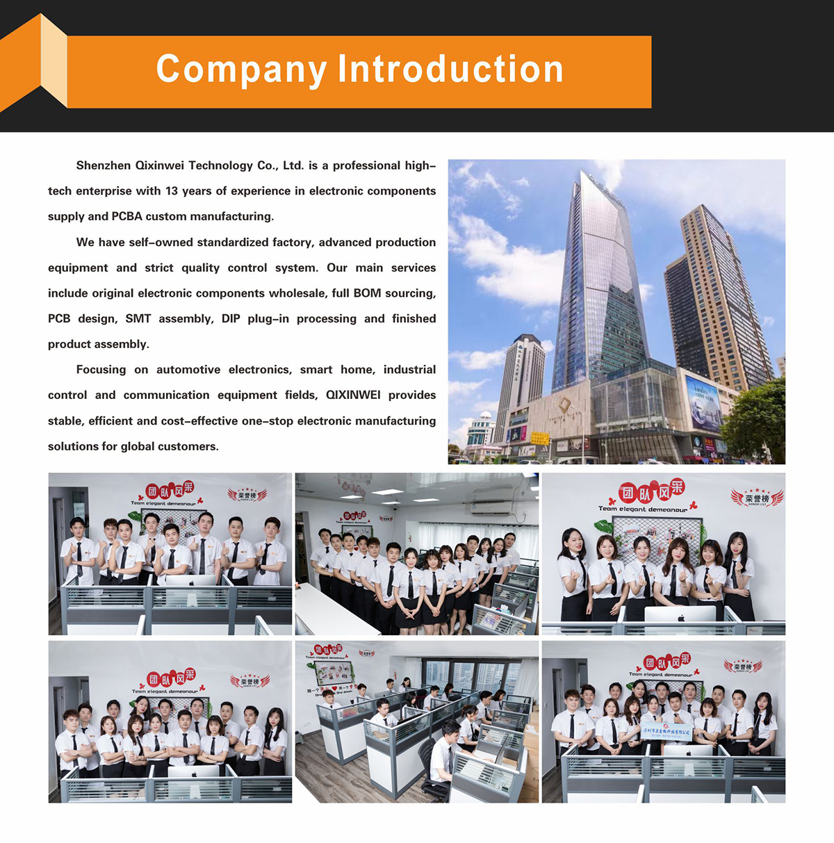
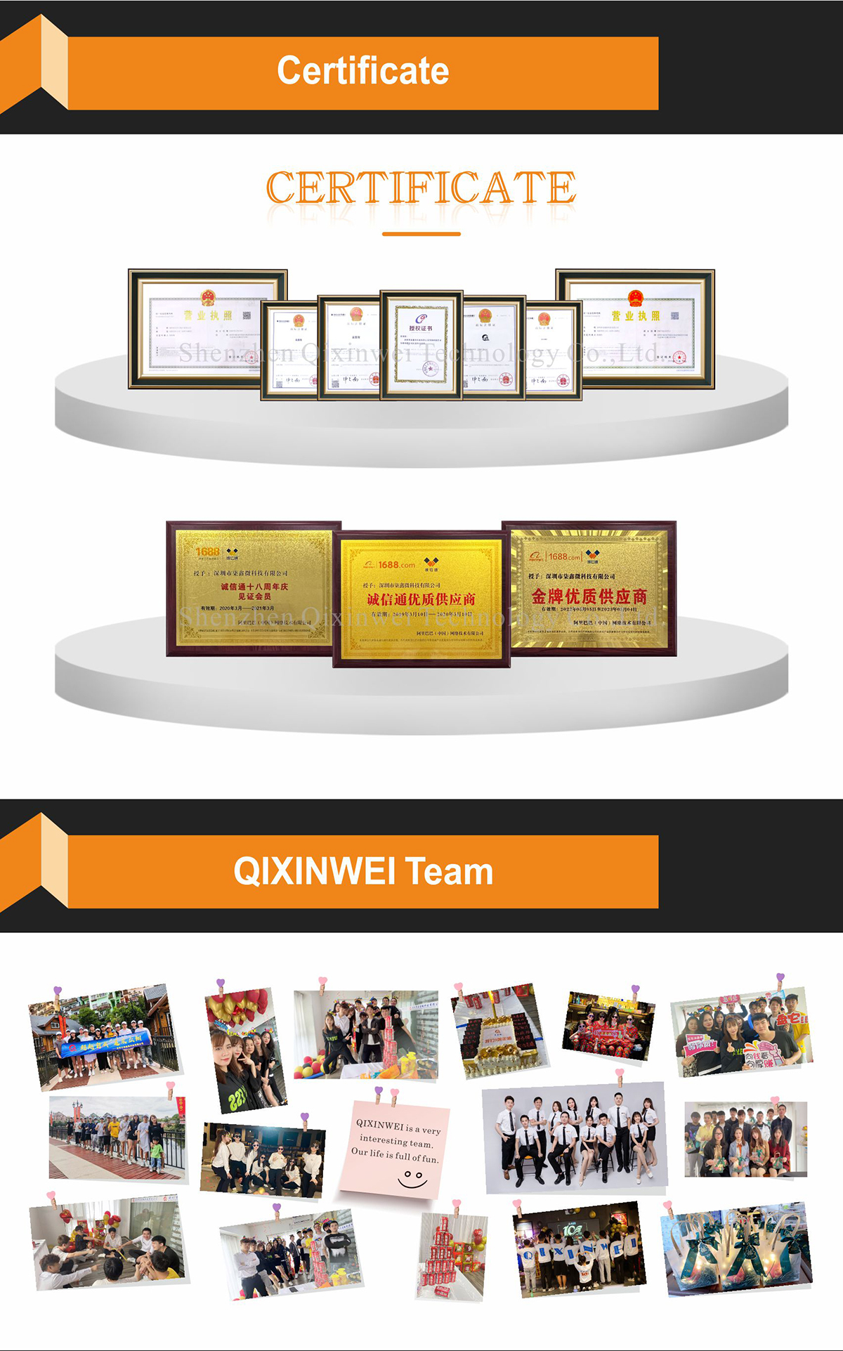
Years of experience in the electronics industry. Trusted by global customers.
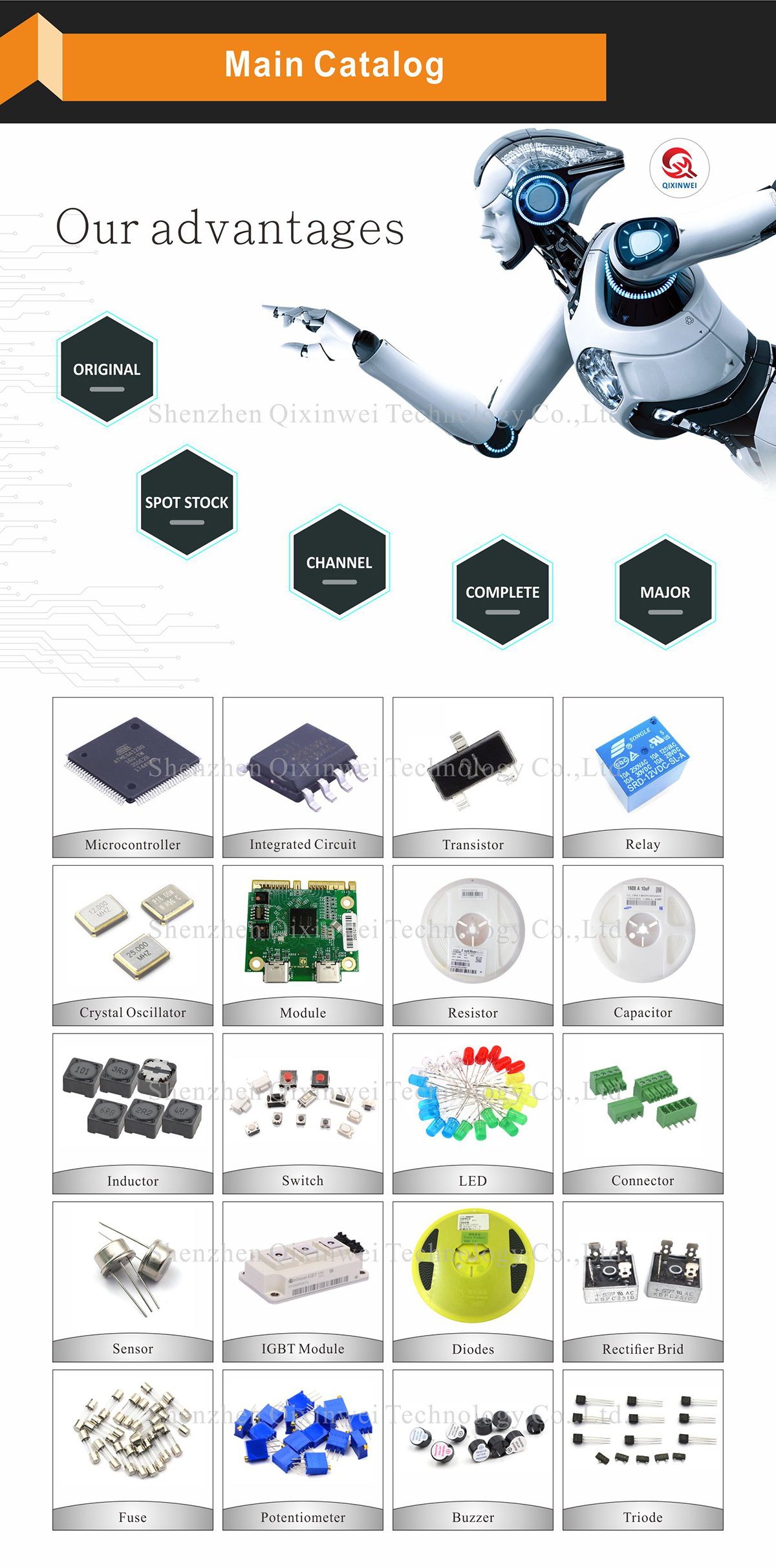
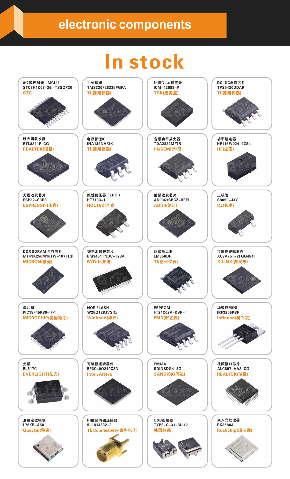
Massive In-Stock Inventory – Ready to ship promptly.
BOM Matching Service – One-stop solution, save time.
PCBA Customization – Professional engineering team creates tailor-made solutions based on your needs.
Cost-Effective & Efficient – Better channel, better cost.
A dedicated team makes your procurement smoother.
Contact us for BOM quotes or PCBA inquiries.







FAQ
1. What is the difference between STM32G474VET3 and STM32G474VET6? What does the “T3” suffix indicate?
Both are identical in processor core (Cortex‑M4 at 170 MHz), Flash (512 KB), SRAM (128 KB), high‑resolution timer (HRTIM), op‑amps, comparators, and all other digital and analog peripherals, and share the same LQFP‑100 package. The only difference is the operating temperature range: the “T3” suffix designates an extended temperature grade, typically ensuring reliable operation from -40 °C to +125 °C, while “T6” is the industrial grade (-40 °C to +85 °C). If your equipment must operate in a high‑temperature environment—such as near an engine, inside a densely packed sealed enclosure, or under direct outdoor sun exposure—the VET3 is the more reliable choice, guaranteeing consistent performance and reliability at extreme temperatures without derating.
2. What practical benefits does the extended temperature range offer? Can the chip truly run at 170 MHz at 125 °C?
The extended temperature grade means the chip has passed more stringent environmental stress screening during production and testing. All electrical parameters and performance specifications published in the datasheet—including 170 MHz operation, 5 Msps ADC accuracy, and op‑amp offset voltages—are guaranteed across the full -40 °C to +125 °C range. For controllers installed in engine compartments, outdoor cabinets, or inside high‑power‑density power modules, this wide‑temperature capability directly impacts long‑term system reliability. You can be confident the system will not experience clock throttling or resets due to high temperatures.
3. Why does this chip have five op‑amps and seven comparators? What can they do in real applications?
The rich analog front‑end is a core strength of the STM32G474 series. The five rail‑to‑rail op‑amps can simultaneously condition multiple current‑sense signals—for example, three‑phase motor currents plus a DC‑link current—or process signals from several thermocouples or pressure sensors, eliminating external op‑amp arrays. The seven ultra‑low‑power comparators can handle multi‑channel over‑current protection, zero‑crossing detection, and voltage‑window monitoring. All these analog blocks are tightly coupled inside the MCU with the HRTIM and DMA to form complete digital control loops, boosting response speed while significantly reducing PCB area and BOM cost.
4. Will the high‑resolution timer (HRTIM) be affected by high temperatures?
No. The HRTIM’s 184 ps resolution is based on digital logic and a PLL, and its accuracy is guaranteed across the entire operating temperature range. In digital power and motor‑control applications, even at an ambient temperature of 125 °C, it can still generate stable, precise, and flexible PWM waveforms supporting topologies such as LLC, half‑bridge, full‑bridge, and phase‑shifted full‑bridge. For automotive DC‑DC converters, on‑board chargers (OBCs), and industrial servo drives that demand high power density and efficiency, the HRTIM is a critical peripheral ensuring control‑loop stability and transient response.
5. Does this chip support FDCAN? How is it used in automotive or industrial communications?
Yes. It integrates up to three FDCAN (Flexible Data‑Rate CAN) controllers, backward‑compatible with CAN 2.0 while supporting data rates up to 5 Mbps and payloads up to 64 bytes. In automotive powertrain domains (engine management, transmission control) and industrial automation, FDCAN can be used for real‑time sensor data sharing, firmware updates, and node health monitoring. Multiple FDCAN channels also enable isolated communication on different bus speeds (e.g., powertrain CAN vs. body CAN) or serve as redundant links to improve system reliability.
6. How does the 512 KB dual‑bank Flash support safe OTA updates?
The dual‑bank architecture allows the current firmware to execute from one bank while a new firmware image is downloaded and verified in the other. An update is completed by simply changing the boot address. If a power loss or verification failure occurs during the update, the hardware automatically rolls back to the original firmware—the device can never be “bricked.” Combined with readout protection (RDP) and the Memory Protection Unit (MPU), you can build a secure and reliable remote firmware update system without relying on an external security chip, making it ideal for equipment installed in hard‑to‑reach locations that are difficult to service in the field.
7. At 125 °C, will the analog performance (e.g., ADC accuracy and op‑amp offset) degrade?
All analog parameters are specified and guaranteed across the full temperature range. The 12‑bit ADC maintains its rated accuracy and 5 Msps sampling rate at 125 °C, and the op‑amp input offset voltage and gain‑bandwidth product remain within their specified limits. To achieve the best performance, however, it is recommended to consider thermal gradients in the PCB layout—for example, route op‑amp differential input pairs close together and away from power devices. Additionally, using the internal voltage reference or an external precision reference can help maintain measurement consistency at high temperatures.
8. What low‑power modes does it support? Will power consumption increase significantly at high temperatures?
The chip supports three low‑power modes: Sleep, Stop, and Standby. In Standby mode, the current can drop to the micro‑amp range while retaining only minimal wake‑up logic. Elevated temperatures do cause some increase in static leakage current, but the STM32G4’s 90 nm low‑power process is designed to suppress leakage. For battery‑powered devices that require long standby times, you can use the RTC and low‑power timers to periodically wake the MCU for measurement and reporting, minimizing average power consumption. Even in a 125 °C environment, long‑term battery operation is achievable with proper capacity and lifetime assessment.
9. What development tools are needed for the STM32G474VET3? Is the code compatible with the standard temperature version?
The code is fully compatible. In STM32CubeMX and STM32CubeIDE, simply select the STM32G474VET3 device; all HAL libraries and firmware code are identical to the VET6 version and require no modification. If you have previously worked with STM32F3 or STM32F4 series, a large portion of HAL code can be reused, with the main adjustments involving analog‑peripheral configuration and pin mapping. ST also provides detailed example projects covering digital power and motor control to help jump‑start development. Debugging and programming use a standard ST‑Link probe.
10. If I later need more memory or a higher core frequency, what upgrade options are available?
If the 512 KB Flash or 128 KB SRAM is insufficient, you can upgrade to STM32G474 models with larger Flash capacities within the same series, or move to the higher‑performance STM32H7 series (such as the STM32H723 or H743), which offer more SRAM and core frequencies up to 550 MHz—also available in extended‑temperature (“3” suffix) variants. Because all these devices belong to the same STM32 ecosystem, code and hardware designs can be highly reused, and migration effort is minimal, with the same wide‑temperature reliability from -40 °C to +125 °C.
- Property:
- Specification
- Product Type:
- Arm Cortex-M4 Mixed-Signal 32-bit MCU
- Brand:
- STMicroelectronics
- Core:
- Cortex-M4 170 MHz (FPU + Math Accelerator)
- Package:
- LQFP-100
- Memory:
- 512 KB Flash, 128 KB SRAM
- Analog:
- 6×Op-Amps, 7×DACs, 7×Comparators, 5×ADCs, 4×Σ-Δ
- HRTIM:
- 12-ch, 184 ps resolution
- Connectivity:
- USB 2.0 FS, CAN FD
- I/Os:
- 86
- Voltage:
- 1.71V–3.6V
- Temperature:
- -40°C to 125°C


