
qixinwei-pcba


STM32G031F6P6 ST Mainstream Arm Cortex-M0+ Low-Power 32-bit MCU 32KB Flash 8KB SRAM ADC Comparator TSSOP-20
STM32G031F6P6 Product Overview
STM32G031F6P6 is a Cortex-M0+ MCU at 64 MHz, TSSOP-20. 32 KB Flash, 8 KB SRAM, 12-bit ADC (10 ch), 1 comparator, LP timers, RTC, 2×USART, 1×SPI, 1×I2C. 18 x 5 V-tolerant I/Os. 2.0–3.6 V, -40–85 °C. Compared to STM32G030F6P6, adds an analog comparator for cost-sensitive compact applications needing analog monitoring.
STM32G031F6P6 Core Features
Core: Cortex-M0+ 64 MHz Memory: 32 KB Flash, 8 KB SRAM Analog: 12-bit ADC (10 ch), 1× comparator Connectivity: 2×USART, 1×SPI, 1×I2C Timers: Advanced PWM, LP timers, RTC I/Os: 18 (5 V-tolerant) Package: TSSOP-20
STM32G031F6P6 Applications
Sensor signal conditioning, home appliances, consumer electronics, IoT nodes, space-constrained general-purpose embedded systems
STM32G031F6P6 Key Advantages
64 MHz Cortex-M0+ with comparator: Efficient performance and analog integration Ultra-small 20-pin package saves board space Wide 2.0–3.6 V for battery operation High value for high-volume analog-sensing designs
Why Choose QIXINWEI
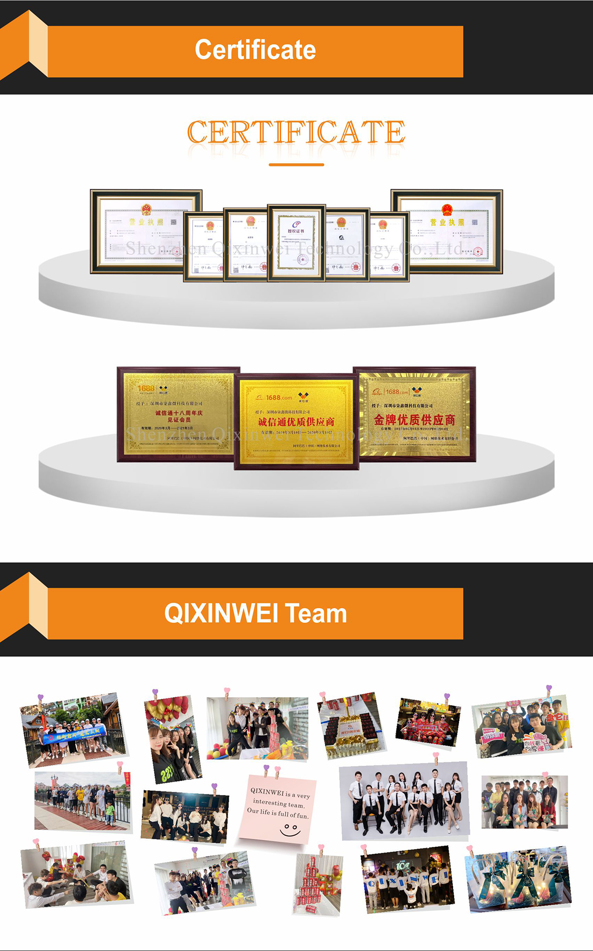
Years of experience in the electronics industry. Trusted by global customers.
Massive In-Stock Inventory – Ready to ship promptly.
BOM Matching Service – One-stop solution, save time.
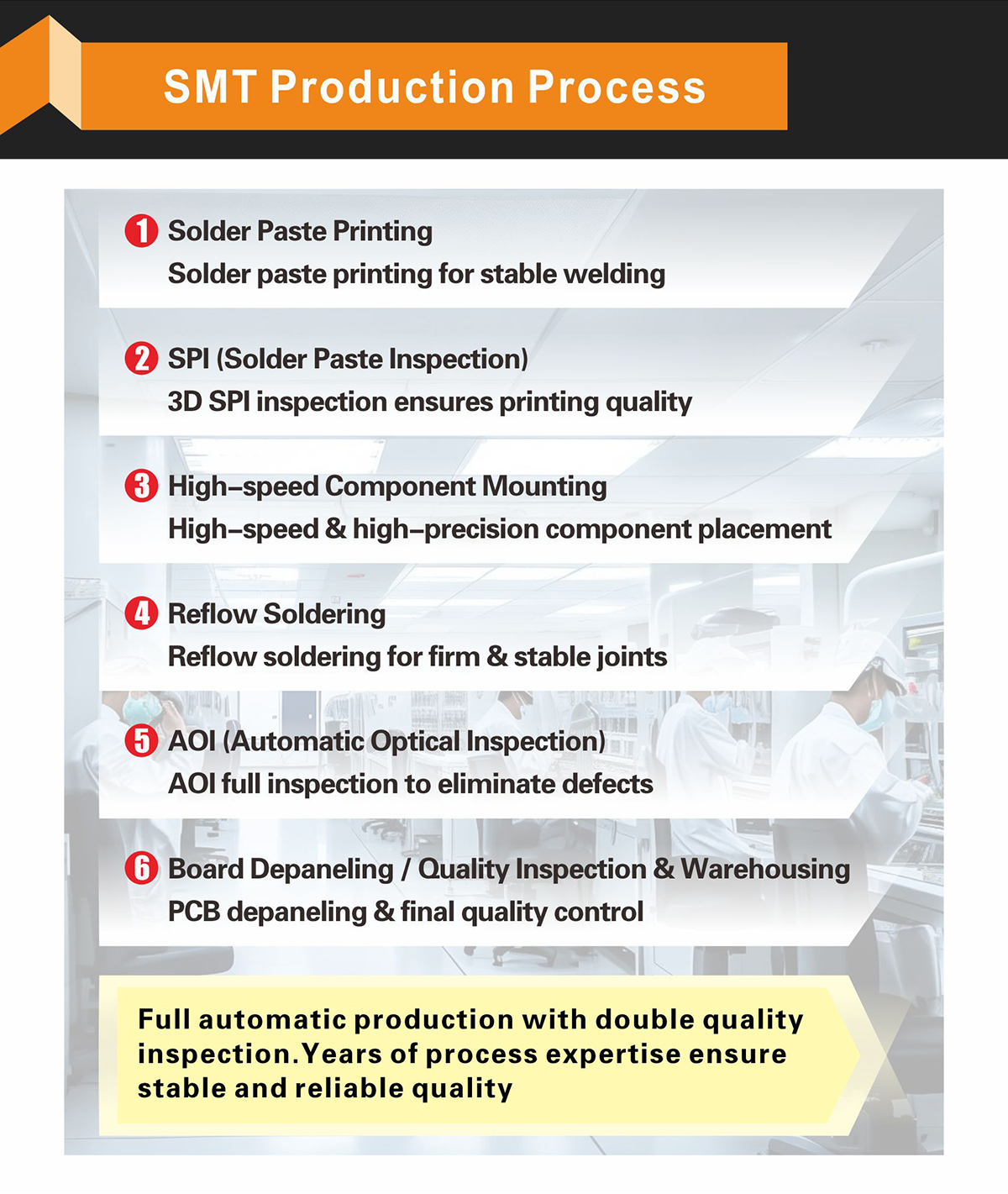
PCBA Customization – Professional engineering team creates tailor-made solutions based on your needs.
Cost-Effective & Efficient – Better channel, better cost.
A dedicated team makes your procurement smoother.
Contact us for BOM quotes or PCBA inquiries.






FAQ
1. What is the STM32G031F6P6, and what advantages does the TSSOP‑20 package offer?
The STM32G031F6P6 is an ultra‑value compact MCU from STMicroelectronics' STM32G0 series, built around a 64 MHz Arm® Cortex®‑M0+ core in a TSSOP‑20 package (6.5 mm × 4.4 mm). It features 32 KB Flash, 8 KB SRAM, two low‑power UARTs, two SPI/I²C interfaces, and a high‑precision 12‑bit ADC. The TSSOP‑20 package’s biggest benefit lies in its exposed leads with a 0.65 mm pitch, which can be easily drag‑soldered with a standard iron. With up to 18 usable I/Os, it provides far more pins than an SO8N package while being much easier to handle than a QFN package, making it ideal for small embedded devices that need moderate peripheral connectivity but demand low cost and simple manufacturing.
2. With only 32 KB Flash and 8 KB SRAM, what kind of programs can I run? Is it enough?
This combination is designed for highly optimized bare‑metal code. The 32 KB Flash can accommodate streamlined sensor drivers, UART/SPI communication stacks, and moderately complex state‑machine logic. The 8 KB SRAM requires careful variable management, but is perfectly adequate for relatively fixed‑function applications—such as environmental sensor data collection, simple motor control, or serial passthrough. If the program size may exceed 32 KB, you can directly upgrade to the pin‑compatible STM32G031F8P6 with 64 KB Flash and zero hardware changes.
3. How does the STM32G031F6P6 differ from the F8P6 (64 KB), and how do I choose based on Flash size?
Both share the same processor core, 8 KB SRAM, two low‑power UARTs, two SPI/I²C interfaces, 12‑bit ADC, and TSSOP‑20 package with fully compatible pinouts. The only difference is on‑chip Flash capacity: F6P6 has 32 KB, while F8P6 has 64 KB. If your firmware is tightly optimized to fit within 32 KB, the F6P6 delivers identical performance and peripherals at a lower cost. If you need more program space or may expand functionality later, the F8P6 is the safer choice. The hardware design can remain unchanged when switching between the two.
4. Does this chip have a USB or CAN interface? What if I need those?
The G031 series does not integrate USB or CAN FD controllers; its communication relies on two low‑power UARTs and two SPI/I²C interfaces. If USB is a must, you can add an external USB‑UART chip such as the CH340. If you require CAN bus, you can upgrade to the pin‑compatible G071F6P6 or G071GBT6 (with a built‑in FDCAN controller), with minimal hardware changes and extensive code reuse.
5. Is the TSSOP‑20 package really easy to solder? How does it compare with QFN and SO8?
Very easy. The TSSOP‑20 has all pins exposed with a 0.65 mm pitch; while slightly denser than the SO8N’s 1.27 mm pitch, it is still very straightforward to drag‑solder with a standard iron and flux—no hot‑air station required. Compared to QFN packages that require reflow soldering and cannot be visually inspected, the TSSOP‑20 offers overwhelming advantages in repairability and low‑volume production. Compared to the SO8N’s 8 pins, the TSSOP‑20 provides far more I/O resources, making it an excellent choice for hobbyists, students, and small teams for prototyping and low‑volume production.
6. What is its power consumption like? Is it suitable for battery‑powered portable devices?
Excellent. The G0 series features a run‑mode current of about 100 µA/MHz and supports multiple low‑power modes—Sleep, Stop, and Standby—with Standby current dropping to the micro‑amp range while retaining the RTC and backup registers. Combined with fast wake‑up times, it can easily achieve years of battery life, making it ideal for wireless sensor nodes, wearables, and outdoor monitoring tools.
7. How accurate is the built‑in 12‑bit ADC? Can it meet typical sensor acquisition needs?
It integrates a 12‑bit successive‑approximation ADC with a maximum sampling rate of 2.5 Msps and up to 16 external input channels. Its accuracy and speed are fully adequate for common sensor signals such as current, voltage, and temperature measurements—often without the need for an external dedicated ADC chip. Multiple ADC channels remain accessible even in the TSSOP‑20 package.
8. What are the main upgrades of the STM32G031F6P6 over the STM32F0 series?
Compared to the STM32F0, the G031 series offers significant improvements: core frequency increases from 48 MHz to 64 MHz; Flash and SRAM capacities are larger (32 KB/8 KB vs. typical 16–32 KB/4–8 KB on the F0); the ADC is more advanced; and overall power management is more refined. It delivers better processing performance and energy efficiency at an entry‑level price, making it an ideal replacement and upgrade for F0 designs.
9. What development tools are needed for the STM32G031F6P6? Is it compatible with the previous STM32 ecosystem?
It is fully compatible with the STM32Cube ecosystem, including the free STM32CubeMX and STM32CubeIDE, along with the STM32CubeG0 firmware package. Code from STM32F0 or F1 projects can be largely reused, with the main adjustments being peripheral configuration and pin mapping. For rapid prototyping, the NUCLEO‑G031K8 board features an LQFP‑32 package with highly compatible pinout and functionality, allowing direct code migration to the TSSOP‑20 chip.
10. If I later need more I/Os or larger memory, what upgrade options are available?
For larger Flash, you can directly upgrade to the same‑package TSSOP‑20 STM32G031F8P6 (64 KB Flash) or G071F6P6/G071F8P6 (128 KB Flash, 36 KB SRAM, adds USB‑C and FDCAN) with zero hardware changes. If you need more I/Os, choose the LQFP‑32 G071K8T6 or the LQFP‑48 G071CBT6. All these upgrades remain within the same STM32Cube ecosystem, allowing extensive code reuse and minimal migration effort.
- Property:
- Specification
- Product Type:
- Arm Cortex-M0+ Low-Power 32-bit MCU
- Brand:
- STMicroelectronics
- Core:
- Cortex-M0+ 64 MHz
- Package:
- TSSOP-20
- Memory:
- 32 KB Flash, 8 KB SRAM
- Analog:
- 12-bit ADC, 1× Comparator
- Connectivity:
- USART, SPI, I2C
- I/Os:
- 18
- Voltage:
- 2.0V–3.6V


