
qixinwei-pcba


STM32F750Z8T6 ST Mainstream Arm Cortex-M7 High-Performance 32-bit MCU 64KB Flash 320KB SRAM LCD-TFT Chrom-ART USB OTG Quad SPI LQFP-144
STM32F750Z8T6 Product Overview
STM32F750Z8T6 is a Cortex-M7 MCU at 216 MHz, LQFP-144. 64 KB Flash, 320 KB SRAM, LCD-TFT controller (up to XGA), Chrom-ART (DMA2D), USB OTG HS/FS (HS needs external ULPI), Quad SPI, 2×SAI, SPDIF-Rx, dual CAN, SDIO, 3×12-bit ADCs (24 ch), 2×12-bit DACs, 17 timers (2× advanced motor control). 114 x 5 V-tolerant I/Os. 1.7–3.6 V, -40–85 °C. Cost-efficient graphics with large SRAM, no Ethernet.
STM32F750Z8T6 Core Features
Core: Cortex-M7 216 MHz, FPU + L1 cache + ART Memory: 64 KB Flash, 320 KB SRAM Display: LCD-TFT (XGA), Chrom-ART (DMA2D) Connectivity: USB OTG HS/FS (HS: external ULPI), SDIO, Quad SPI, 2×SAI, SPDIF-Rx, Dual CAN 2.0B, 4×USART+4×UART, 6×SPI/I2S, 3×I2C Analog: 3×12-bit ADCs (24 ch), 2×12-bit DACs Timers: 17 (2× motor control PWM/deadtime, 10× GP, 2× basic, 2× WDT) I/Os: 114 (5 V-tolerant) Package: LQFP-144
STM32F750Z8T6 Applications
Cost-sensitive HMI, industrial displays, motor control, USB devices, audio interfaces, IoT endpoints
STM32F750Z8T6 Key Advantages
320 KB SRAM + Chrom-ART: Smooth graphics with large buffer 216 MHz Cortex-M7: High real-time performance LCD-TFT direct drive, no Ethernet, cost-optimized Quad SPI + SAI + Dual CAN: Rich data interfaces 114 I/Os, LQFP-144 package
Why Choose QIXINWEI
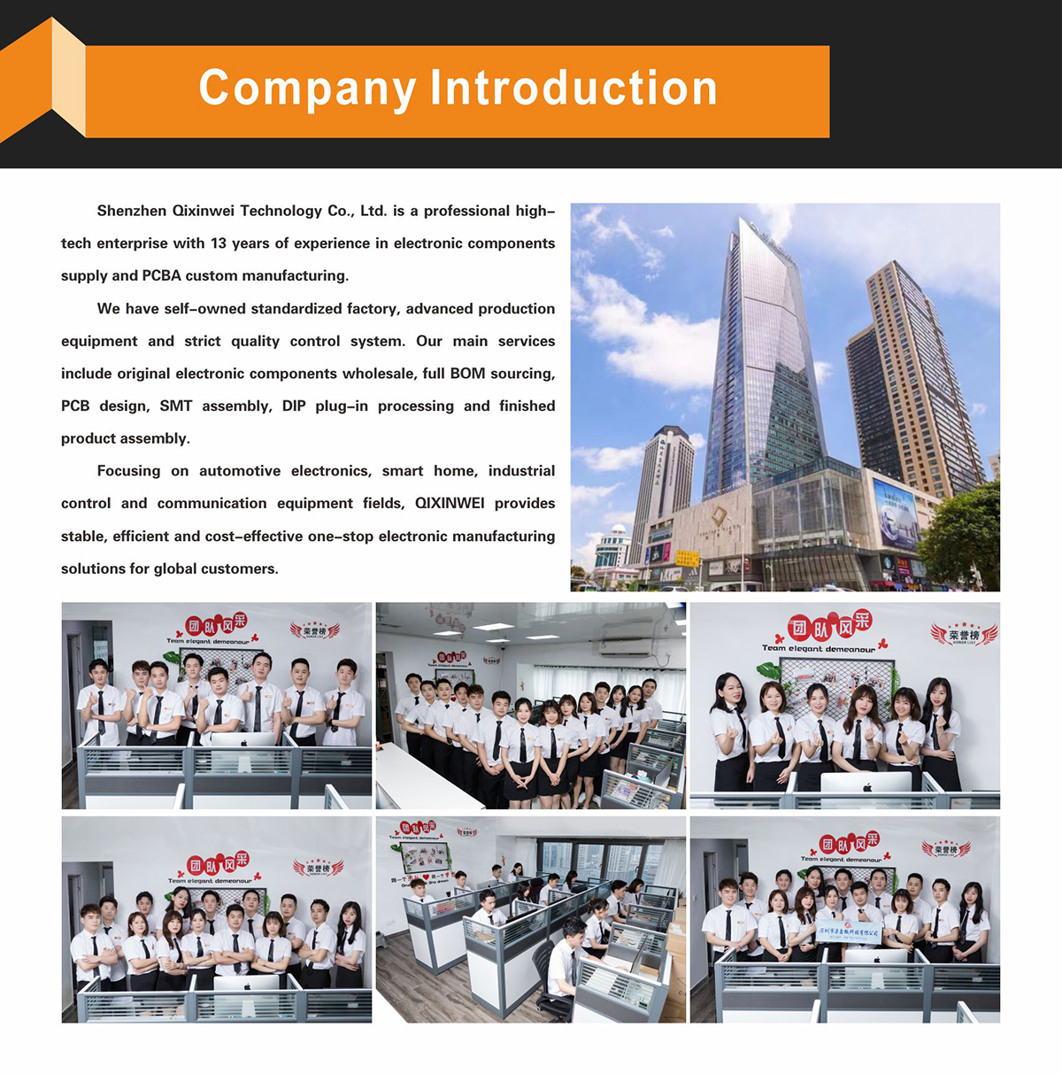
Years of experience in the electronics industry. Trusted by global customers.
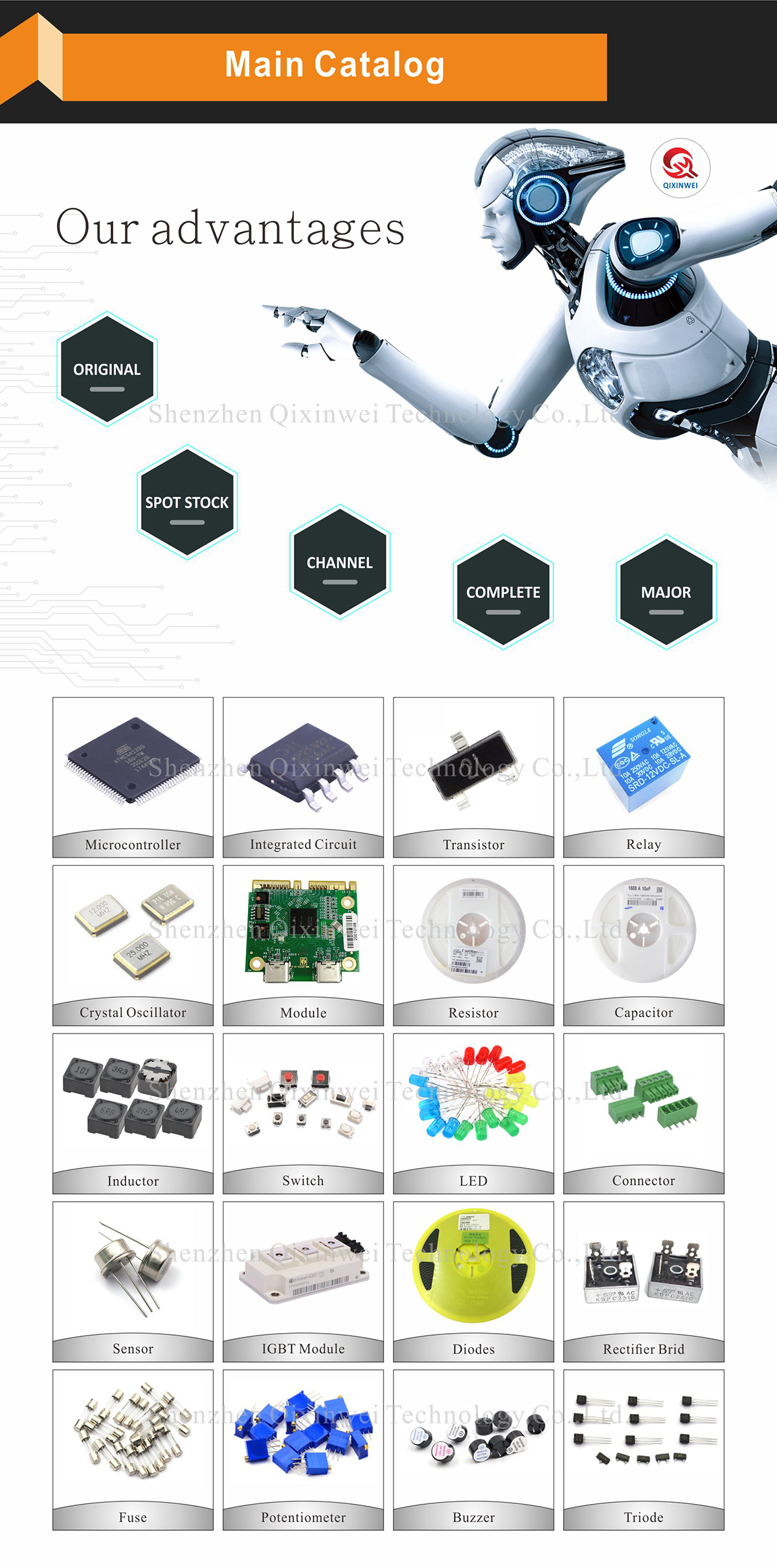
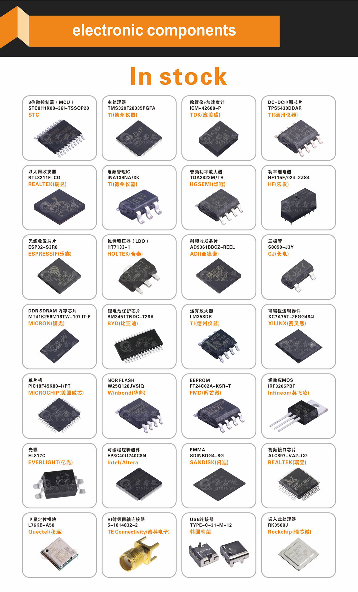
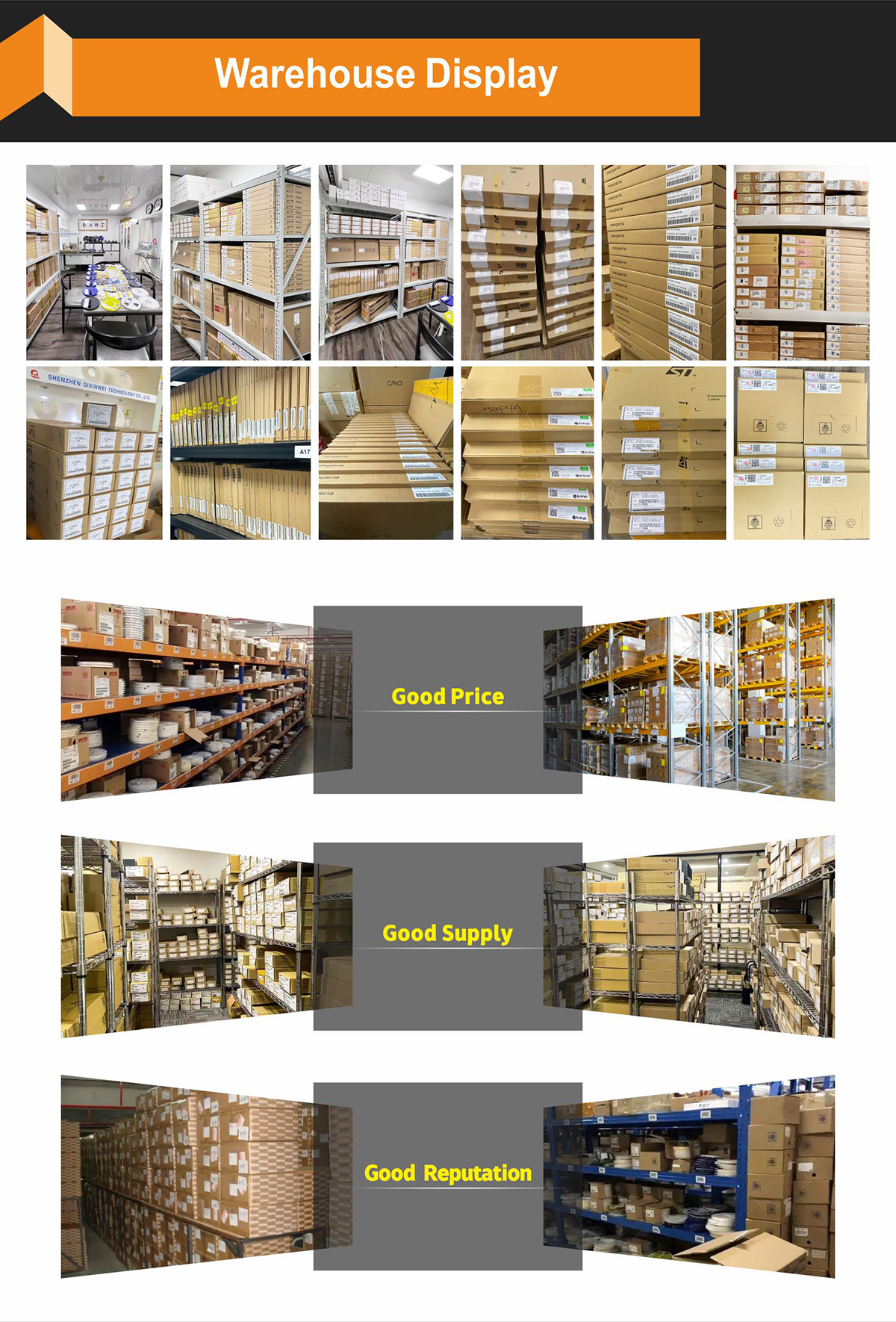
Massive In-Stock Inventory – Ready to ship promptly.
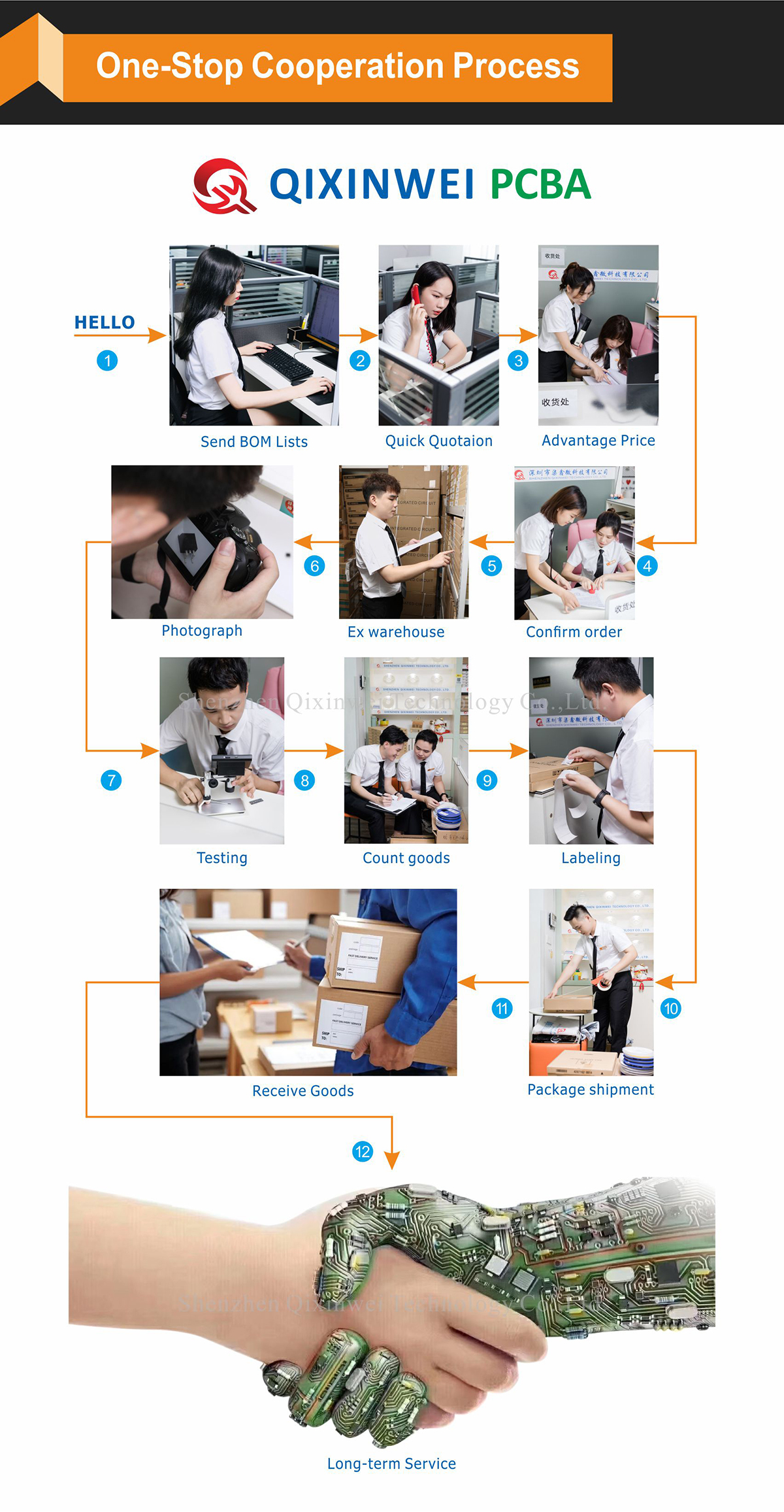
BOM Matching Service – One-stop solution, save time.
PCBA Customization – Professional engineering team creates tailor-made solutions based on your needs.
Cost-Effective & Efficient – Better channel, better cost.
A dedicated team makes your procurement smoother.
Contact us for BOM quotes or PCBA inquiries.

FAQ:
What is the STM32F750Z8T6 and why does it only have 64 KB of internal Flash?
The STM32F750Z8T6 is a Cortex‑M7 microcontroller running at 216 MHz with a TFT‑LCD controller, Chrom‑ART accelerator, and 320 KB of SRAM. The small 64‑KB internal Flash is deliberately designed to hold only the boot code and critical interrupt vectors, while the main application is stored and executed directly from a low‑cost external Quad‑SPI Flash via the memory‑mapped XIP (eXecute In Place) mode. This architecture drastically reduces system cost for feature‑rich graphical applications.How can I run a large application on the STM32F750 if it has so little internal Flash?
You place your firmware in an external QSPI Flash (e.g., 16 MB or larger). The F750 boots from the internal Flash, which configures the QSPI peripheral into memory‑mapped mode and then jumps to the application stored in the external Flash. The Cortex‑M7 can then fetch and execute code directly from the QSPI memory through a 64‑KB cache, providing performance very close to internal Flash execution for most code.What is the boot process for STM32F750 when using external QSPI Flash? How do I set it up?
A typical scheme places a small bootloader or startup code in the internal 64‑KB Flash. This startup code initializes the QSPI interface, maps the external Flash to the memory space (usually starting at 0x90000000), and then sets the vector table address to the external Flash before jumping to the application. STM32CubeMX can generate the necessary startup code, and you can select “External Loader” in the programming options to write the external Flash.Does the STM32F750Z8T6 have the same graphics capabilities as the STM32F746? Can it drive a high‑resolution TFT?
Yes. The F750 integrates the exact same TFT‑LCD controller and Chrom‑ART (DMA2D) accelerator as the STM32F746. It can drive displays up to XGA (1024×768) with 24‑bit color. The Chrom‑ART hardware handles pixel blending, format conversion, and copying, delivering smooth GUI performance at high resolutions. The only difference is the memory architecture—the F750 relies on external Flash for code storage.How can the 64‑KB internal Flash be used effectively in a real design?
The internal Flash is ideal for the initial bootloader, secure keys, calibration data, or a failsafe recovery image. Since it is the only memory guaranteed to be present at power‑up before QSPI is configured, it can also store a simple diagnostic application that runs if the external Flash content is corrupted, allowing a system to be re‑programmed without requiring a JTAG/SWD connection.How does the STM32F750Z8T6 compare with the STM32F746? Is it a drop‑in replacement?
The F750 and F746 share the same LQFP‑144 package, identical I/O multiplexing, and the same graphics engine. The F746 has 1 MB of internal Flash, while the F750 replaces it with a QSPI XIP scheme using only 64 KB of internal Flash. In many designs, the F750 can be a lower‑cost alternative to the F746 when your firmware size exceeds 1 MB and you would have needed external Flash anyway. Migration requires re‑linking the application for the QSPI memory map and adding an external Flash chip.What is the real‑time performance penalty when executing code from an external QSPI Flash?
The F750 uses a 64‑KB L1 cache and an ART accelerator to buffer QSPI fetches. For most sequential code, the cache hit rate is very high (often >95%), making execution nearly as fast as internal Flash. Performance‑critical interrupt service routines and tight loops can optionally be placed in the internal 64‑KB Flash or in SRAM to guarantee deterministic timing. For a GUI application, the Chrom‑ART and LTDC operate independently, so QSPI code execution rarely affects screen refresh.How is the 320‑KB SRAM organized, and can it hold a complete frame buffer?
The 320 KB of on‑chip RAM is divided into 256 KB of general‑purpose SRAM and 64 KB of DTCM (Data Tightly Coupled Memory). For a display at 800×480 in 16‑bit color, a single frame buffer needs about 768 KB, which exceeds the internal SRAM. Most designs add a small external SDRAM (e.g., 8‑16 MB) connected via the flexible memory controller to hold the frame buffer and large graphics assets, while the internal SRAM handles the application stack, heap, and real‑time data.What development tools support the STM32F750Z8T6, and how do I program the external Flash?
STM32CubeIDE, Keil MDK, and IAR EWARM all fully support the F750. To program the external QSPI Flash, you need an external loader (a small piece of software that runs on the target and writes the Flash). STM32CubeProgrammer and most IDEs can use these loaders, and you can generate them through STM32CubeMX. Once set up, the IDE will automatically erase and program the external Flash whenever you flash the target, just as it does for internal memory.What are the ideal applications for the STM32F750Z8T6, and what are its main advantages?
It is perfect for cost‑sensitive embedded GUI products that need a high‑resolution color display: smart home control panels, industrial HMI terminals, IoT wall pads, and portable medical devices. The main advantage is that the QSPI XIP architecture allows you to use a very cheap external Flash instead of paying for a large on‑chip Flash, significantly lowering the overall system cost while keeping the full graphics and processing power of the STM32F7 series.
- Property:
- Specification
- Product Type:
- Arm Cortex-M7 High-Performance 32-bit MCU
- Brand:
- STMicroelectronics
- Core:
- Cortex-M7 216 MHz (FPU + L1 cache)
- Package:
- LQFP-144
- Memory:
- 64 KB Flash, 320 KB SRAM
- Display:
- LCD-TFT, Chrom-ART
- Connectivity:
- USB OTG, Quad SPI, SAI, Dual CAN
- Analog:
- 3×12-bit ADCs, 2×12-bit DACs
- I/Os:
- 114
- Voltage:
- 1.7V–3.6V


