
qixinwei-pcba


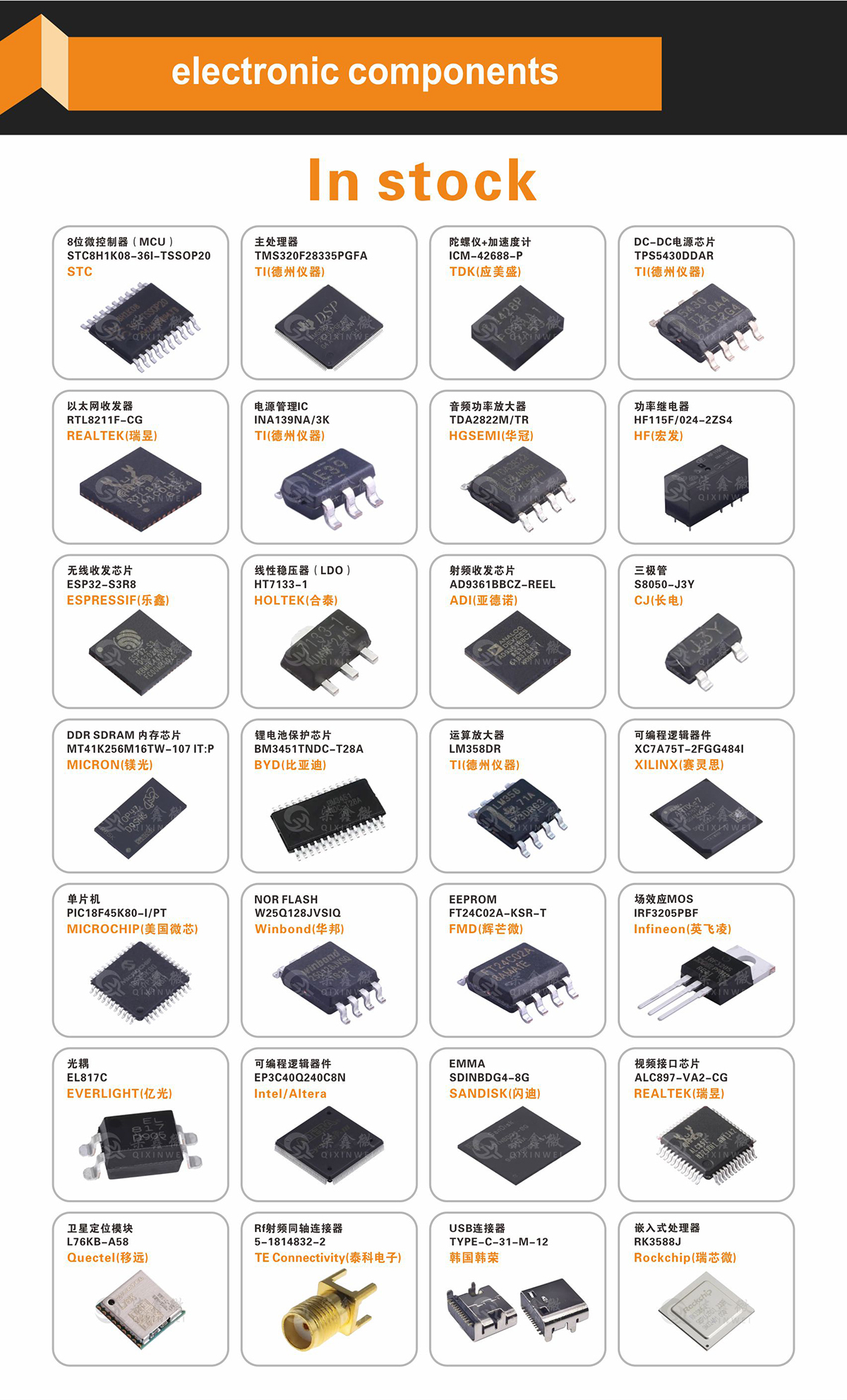
STM32F415RGT6 ST Mainstream Arm Cortex-M4 High-Performance 32-bit MCU 1MB Flash 168MHz FPU USB OTG SDIO DCMI Crypto LQFP-64
STM32F415RGT6 Product Overview
The STM32F415RGT6 is a Cortex-M4 high-performance MCU from STMicroelectronics in an LQFP-64 package. It runs at 168 MHz with FPU and ART Accelerator. It integrates 1 MB Flash, 192 KB SRAM, USB 2.0 OTG (FS/HS), SDIO, camera interface (DCMI), hardware crypto/HASH processor (AES 128/192/256, 3DES, HASH/MD5/SHA-1, RNG), two 12-bit DACs, three 12-bit ADCs (16ch, up to 7.2 MSPS in triple-interleaved mode), up to 17 timers (incl. 2 advanced motor control PWM/deadtime). 51 I/Os, all 5 V-tolerant. Supply 1.8–3.6 V, -40–85 °C. Core specifications are identical to the STM32F405RGT6, with the addition of a hardware crypto/HASH engine, providing hardware-level encryption support for applications requiring data security and integrity verification. It is an ideal choice that combines high performance and data security in an LQFP-64 package.
STM32F415RGT6 Core Features
Core: Arm Cortex-M4 168 MHz + FPU + ART Accelerator Memory: 1 MB Flash, 192 KB SRAM USB 2.0 OTG: FS + HS, FS on-chip PHY, HS requires external ULPI SDIO + HW Crypto: SD/MMC interface; AES 128/192/256, 3DES, HASH (MD5, SHA-1), RNG Camera Interface: 8–14-bit parallel DCMI 3×12-bit ADCs: 16 channels, 2.4 MSPS (up to 7.2 MSPS in triple-interleaved mode) 2×12-bit DACs: Buffered output Timers: Up to 17 (2× motor control PWM/deadtime/emergency stop, 12× 16-bit GP/quadrature encoder, 2× basic, 2× watchdogs, SysTick) Communication Interfaces: 4×USART + 2×UART (ISO7816/LIN/IrDA), 3×SPI (30 Mbit/s), 2×I2S, 3×I2C (SMBus), USB OTG, SDIO I/Os: 51, all 5 V-tolerant Low Power: Sleep/Stop/Standby, VBAT backup RTC Package: LQFP-64 (10×10×1.4 mm)
STM32F415RGT6 Applications
Industrial: PLCs, inverters, precision motor drives Motor Control: Dual-motor FOC, servo drives, pumps Image Capture: Simple camera monitoring, barcode scanning, industrial vision Security Applications: IoT security, payment terminals, data integrity verification Consumer: Drone flight controllers, game controllers, high-end remote controls Portable Medical Devices
STM32F415RGT6 Key Advantages
168 MHz Cortex-M4 + FPU: Strongest performance in this package class for complex DSP and floating-point operations Hardware Crypto Engine: AES/3DES/HASH/RNG for hardware-level data security and integrity 192 KB SRAM + 1 MB Flash: Ample memory for large firmware and complex algorithms DCMI Camera Interface: Supports CMOS sensors for image capture and vision applications Dual DACs + 3 ADCs: Comprehensive analog functions with multi-channel synchronous acquisition 17 Timers (incl. 2 Motor Control): Supports dual-motor FOC Mature STM32 Ecosystem: CubeIDE/CubeMX/HAL/LL
Why Choose QIXINWEI
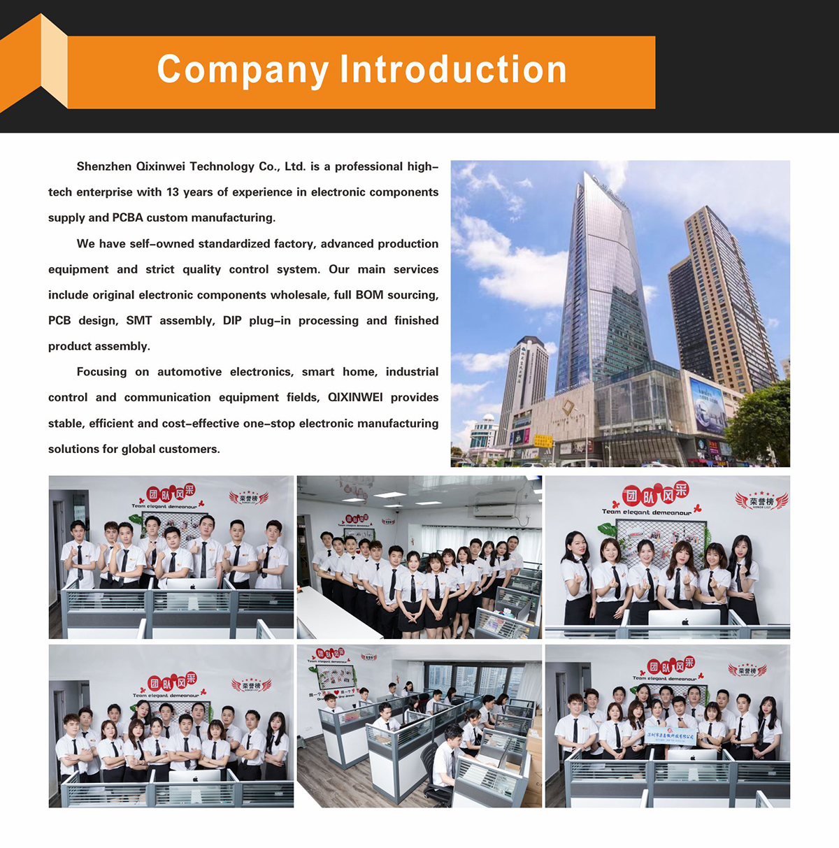
Years of experience in the electronics industry. Trusted by global customers.
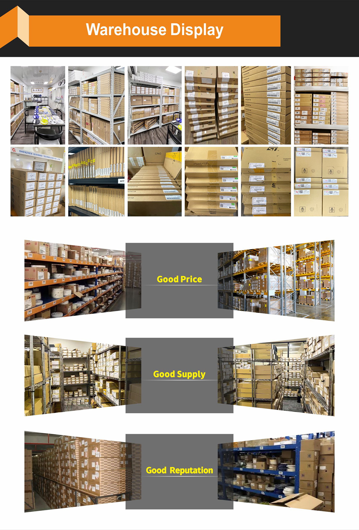
Massive In-Stock Inventory – Ready to ship promptly.
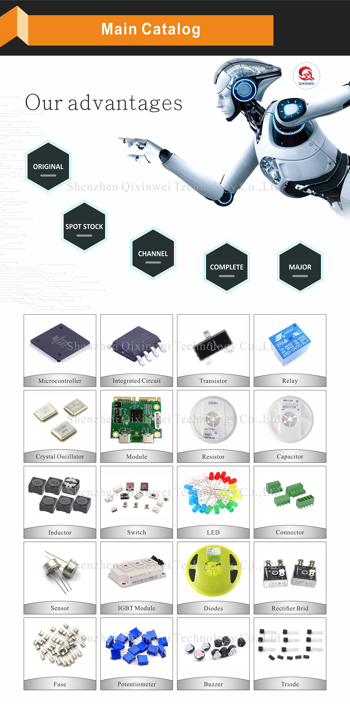
BOM Matching Service – One-stop solution, save time.
PCBA Customization – Professional engineering team creates tailor-made solutions based on your needs.
Cost-Effective & Efficient – Better channel, better cost.
A dedicated team makes your procurement smoother.
Contact us for BOM quotes or PCBA inquiries.

FAQ:
What is the STM32F415RGT6 and how does it differ from the STM32F405 and F407?
The STM32F415RGT6 is a 168 MHz Cortex‑M4 microcontroller with 1 MB Flash, 192 KB SRAM, and a hardware cryptographic accelerator (AES, DES, 3DES, hash) in a compact LQFP‑64 package. It sits between the STM32F405 (no crypto) and the STM32F417 (crypto + Ethernet). The F415 provides the same crypto engine as the F417 and the same 1 MB Flash density, but in a smaller 64‑pin body that is perfect for space‑sensitive IoT nodes, secure serial interfaces, and portable medical devices.How much Flash and SRAM does the STM32F415RGT6 offer, and is 1 MB enough for a real‑time OS and secure communication?
The chip provides 1 MB of internal Flash and 192 KB of SRAM (128 KB general‑purpose + 64 KB CCM). The large Flash easily accommodates a real‑time OS, a TCP/IP stack, mbedTLS with hardware acceleration, and a complex application. Many secure IoT gateways, industrial sensors, and USB‑based data loggers fit comfortably within this memory envelope, often leaving room for future updates or an A/B firmware slot.What hardware cryptographic engines does the STM32F415RGT6 integrate? Can it perform AES‑256 on the fly?
The F415RGT6 includes a dedicated crypto processor that supports AES‑128, AES‑192, and AES‑256 in ECB, CBC, and CTR modes, as well as triple DES, MD5, SHA‑1, and a true random number generator. With DMA, you can encrypt and decrypt data on the fly without loading the 168 MHz CPU, making it ideal for secure boot, TLS/SSL communication, and protected firmware updates.Is the STM32F415RGT6 a good upgrade from the STM32F405? What are the additional benefits?
Yes, it is a direct upgrade. The F415RGT6 adds hardware cryptographic acceleration while keeping the same LQFP‑64 package, identical pin‑out, CPU speed, and memory sizes as the STM32F405. You can drop it into an existing F405 design, enable the crypto module, and immediately gain hardware‑accelerated encryption for TLS, secure boot, and AES‑256, without any PCB changes.Can the LQFP‑64 package handle multiple serial peripherals? How many UART, SPI, and I2C ports are available?
The LQFP‑64 provides up to 51 I/O pins. The chip itself offers 6 USART/UART, 3 SPI/I2S, and 3 I2C interfaces. With careful planning, you can typically run 4 UARTs, 2 SPIs, and 2 I2Cs concurrently alongside a few GPIOs and an SDIO interface. STM32CubeMX helps you avoid pin conflicts while maximising the available serial connectivity.Does the STM32F415RGT6 support USB high‑speed, or only full‑speed?
It includes a full‑speed USB OTG controller with an integrated on‑chip PHY, enabling direct USB FS device operation without extra components. For high‑speed (480 Mbps), an external ULPI PHY must be connected to the dedicated ULPI pins. The chip supports both modes, allowing you to start with FS and later add an HS PHY for higher bandwidth applications.How is the 192 KB SRAM organised, and what is the CCM memory used for?
The SRAM consists of 128 KB of general‑purpose system SRAM and 64 KB of core‑coupled memory (CCM). The CCM is directly attached to the CPU data bus and provides zero‑wait‑state access, making it perfect for the stack, real‑time control data, and frequent lookup tables. However, CCM cannot be accessed by DMA, so all DMA‑based buffers should be placed in the 128 KB system SRAM.Can I implement secure over‑the‑air (OTA) firmware updates with the STM32F415RGT6's 1 MB Flash?
Yes. You can partition the 1 MB Flash into a secure bootloader, an active application, and a download buffer, or use two application slots for A/B updates. The hardware crypto engine verifies the firmware signature before the new image is committed. The on‑chip SRAM buffers the encrypted payload during download, ensuring a safe and authenticated update process even on a single‑bank Flash.What development tools support the STM32F415RGT6? Is there a suitable Nucleo board?
All mainstream IDEs—free STM32CubeIDE, Keil MDK, and IAR EWARM—fully support the chip. While no Nucleo‑64 board uses the exact STM32F415RGT6, the NUCLEO‑F446RE (also LQFP‑64) or the STM32F4 Discovery boards can be used for initial firmware development. You then migrate to the F415 by enabling the crypto module in CubeMX and adjusting the linker script for the 1 MB Flash.What are the most typical applications for the STM32F415RGT6, given its compact size and crypto features?
It is ideal for secure IoT sensor nodes, encrypted USB dongles, portable medical instruments, industrial communication modules (CAN‑to‑USB, Modbus‑to‑Ethernet), and any space‑constrained design that requires strong hardware security, generous memory, and a proven Cortex‑M4 ecosystem in a tiny, easy‑to‑manufacture LQFP‑64 package.
- Product Type:
- Mainstream Arm Cortex-M4 High-Performance 32-bit MCU
- Brand:
- STMicroelectronics
- Core:
- Arm Cortex-M4 168MHz (FPU + ART Accelerator)
- Package:
- LQFP-64 (10×10×1.4mm)
- Memory:
- 1MB Flash, 192KB SRAM
- Peripherals:
- USB 2.0 OTG FS/HS, SDIO, DCMI, HW Crypto (AES/3DES/HASH/RNG), 3×12-bit ADCs (16ch/2.4MSPS), 2×12-bit DACs, 2× Motor control PWM (deadtime), 12×16-bit GP timers (quadrature encoder), Calendar RTC
- Interfaces:
- 4×USART, 2×UART, 3×SPI (30Mbit/s), 2×I2S, 3×I2C (SMBus)
- I/Os:
- 51
- Voltage:
- 1.8V~3.6V
- Temperature:
- -40°C~85°C


