
qixinwei-pcba


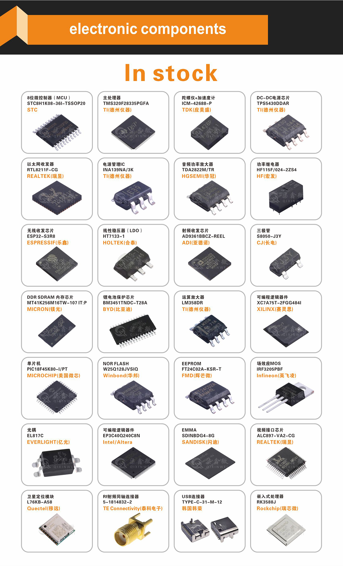
STM32F407ZET6 ST Mainstream Arm Cortex-M4 High-Performance 32-bit MCU 512KB Flash 168MHz FPU Ethernet USB OTG DCMI LQFP-144
STM32F407ZET6 Product Overview
The STM32F407ZET6 is a Cortex-M4 high-performance MCU from STMicroelectronics in an LQFP-144 package. It runs at 168 MHz with FPU and ART Accelerator. It integrates 512 KB Flash, 192 KB SRAM (incl. 64 KB CCM), Ethernet 10/100 MAC (IEEE 1588 PTP, MII/RMII), USB 2.0 OTG (FS/HS, FS on-chip PHY), camera interface (DCMI), hardware crypto/HASH processor, two 12-bit DACs, three 12-bit ADCs (24ch, up to 7.2 MSPS in triple-interleaved mode), up to 17 timers (incl. 2 advanced motor control PWM/deadtime). 114 I/Os, all 5 V-tolerant. Supply 1.8–3.6 V, -40–85 °C. Core specifications are identical to the STM32F407VET6 (LQFP-100, 82 I/Os), with the package upgraded to LQFP-144 to provide richer I/O resources. Compared to the STM32F405ZGT6 (LQFP-144, without Ethernet), this model integrates an Ethernet MAC interface, making it a cost-effective choice that combines network communication with rich peripherals in an LQFP-144 package.
STM32F407ZET6 Core Features
Core: Arm Cortex-M4 168 MHz + FPU + ART Accelerator Memory: 512 KB Flash, 192 KB SRAM (incl. 64 KB CCM) Ethernet MAC: 10/100 Mbit/s, IEEE 1588 PTP hardware support, MII/RMII USB 2.0 OTG: FS + HS, FS on-chip PHY, HS requires external ULPI SDIO + HW Crypto: SD/MMC interface; AES 128/192/256, 3DES, HASH (MD5, SHA-1), RNG Camera Interface: 8–14-bit parallel DCMI 3×12-bit ADCs: 24 channels, 2.4 MSPS (up to 7.2 MSPS in triple-interleaved mode) 2×12-bit DACs: Buffered output Timers: Up to 17 (2× motor control PWM/deadtime/emergency stop, 12× 16-bit GP/quadrature encoder, 2× basic, 2× watchdogs, SysTick) Communication Interfaces: 4×USART + 2×UART (ISO7816/LIN/IrDA), 3×SPI (30 Mbit/s), 2×I2S, 3×I2C (SMBus), USB OTG, SDIO, Ethernet I/Os: 114, all 5 V-tolerant Low Power: Sleep/Stop/Standby, VBAT backup RTC Package: LQFP-144 (20×20×1.4 mm)
STM32F407ZET6 Applications
Industrial: PLCs, inverters, precision motor drives, industrial Ethernet gateways Motor Control: Dual-motor FOC, servo drives, pumps Image Capture: Simple camera monitoring, barcode scanning, industrial vision Network Communication: Ethernet control nodes, IoT gateways Consumer: Drone flight controllers, game controllers, high-end remote controls Security Applications: IoT security, payment terminals Portable Medical Devices
STM32F407ZET6 Key Advantages
168 MHz Cortex-M4 + FPU: Strongest performance in this series for complex DSP and floating-point operations Ethernet + DCMI + Crypto Engine: Network communication, image capture, and data security in a 144-pin package 192 KB SRAM + 512 KB Flash: Large memory capacity for complex application demands Dual DACs + 3 ADCs: Comprehensive analog functions with multi-channel synchronous acquisition 17 Timers (incl. 2 Motor Control): Supports dual-motor FOC Mature STM32 Ecosystem: CubeIDE/CubeMX/HAL/LL
Why Choose QIXINWEI
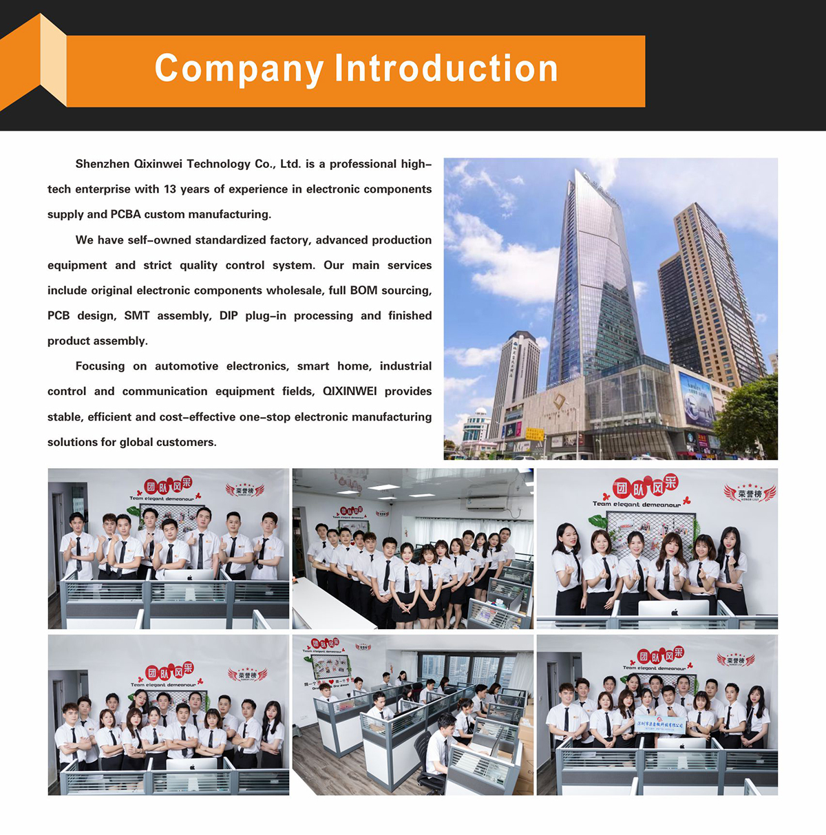
Years of experience in the electronics industry. Trusted by global customers.
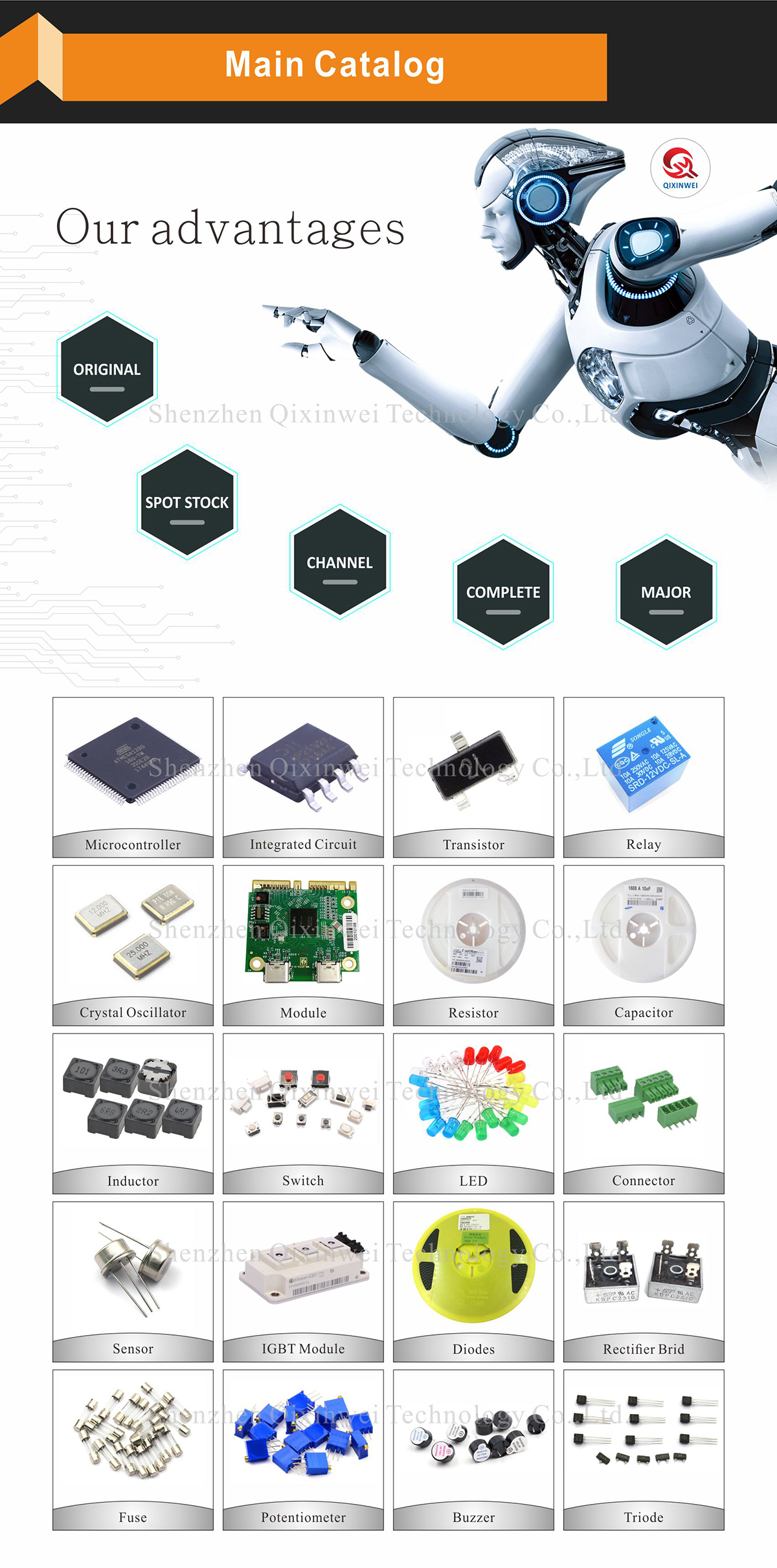
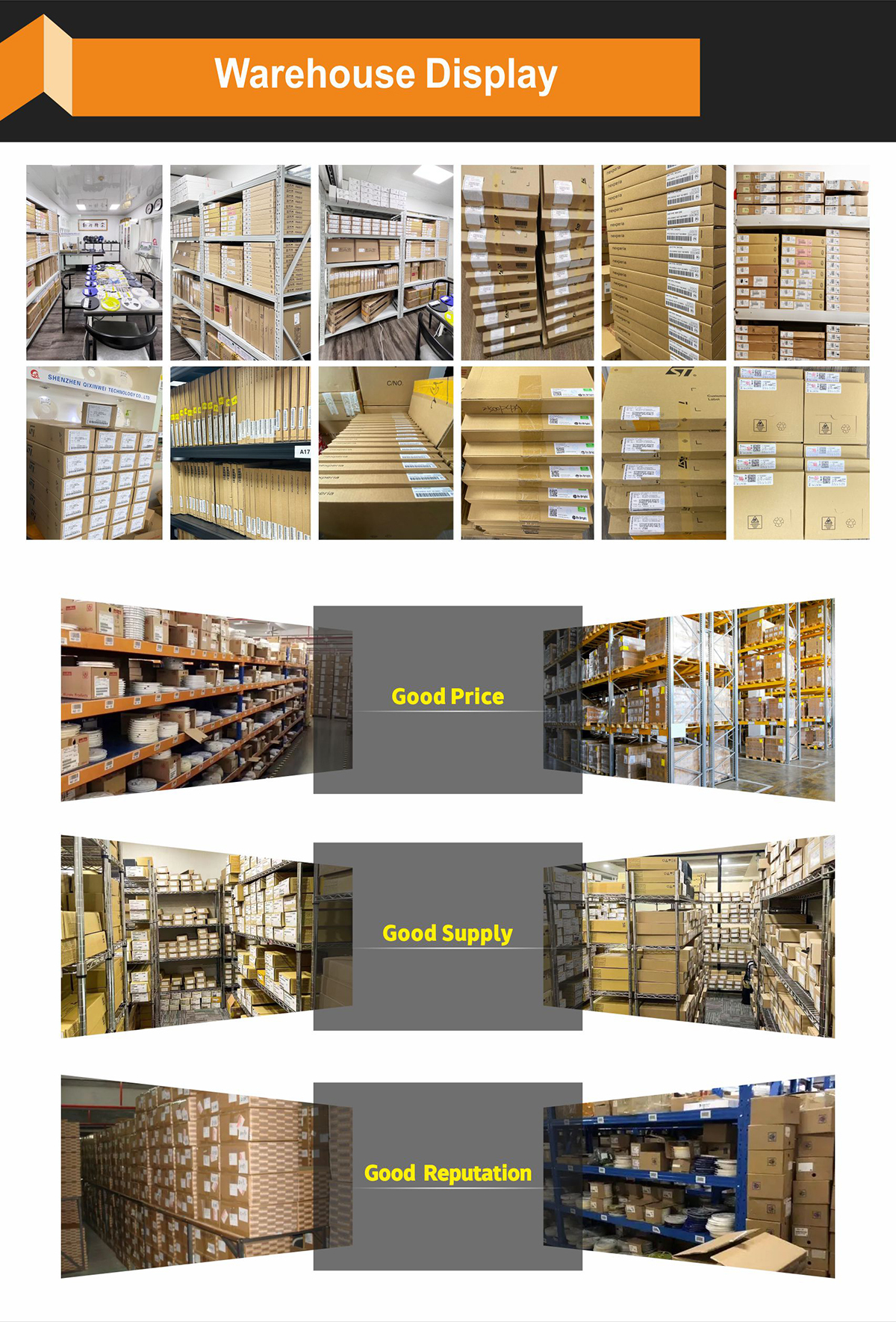
Massive In-Stock Inventory – Ready to ship promptly.
BOM Matching Service – One-stop solution, save time.
PCBA Customization – Professional engineering team creates tailor-made solutions based on your needs.
Cost-Effective & Efficient – Better channel, better cost.
A dedicated team makes your procurement smoother.
Contact us for BOM quotes or PCBA inquiries.

FAQ:
What is the STM32F407ZET6 and how does it differ from the STM32F407ZGT6?
The STM32F407ZET6 is a 168 MHz Arm Cortex‑M4F microcontroller with 512 KB Flash, 192 KB SRAM, a DCMI camera interface, a 10/100 Ethernet MAC, USB OTG HS/FS, dual CAN, and an FMC supporting SDRAM, all in an LQFP‑144 package. The only difference from the ZGT6 is Flash size: the ZET6 has 512 KB while the ZGT6 offers 1 MB. All other features—CPU speed, SRAM, peripherals, and pin‑out—are identical. Choose the ZET6 when your firmware fits within 512 KB and you want a cost‑optimised entry into the STM32F407 line with the same I/O and connectivity.Is 512 KB of Flash enough for a real‑time OS, Ethernet, and a camera application? What fits in this space?
Absolutely. A typical design with FreeRTOS, LwIP, a USB device stack, a DCMI camera driver, and basic image processing easily fits within 400–480 KB, leaving room for application code. Many industrial IP cameras, networked sensors, and Ethernet‑to‑CAN gateways operate comfortably with 512 KB of Flash. If your code outgrows this limit, the pin‑compatible ZGT6 (1 MB) provides a direct drop‑in upgrade.How does the STM32F407ZET6 compare with the STM32F407VET6? When should I pick the 144‑pin version?
The VET6 is the 100‑pin LQFP variant with the same 512 KB Flash and 192 KB SRAM, but it offers fewer I/Os (82 vs 114). The ZET6 adds more pins for a full 32‑bit SDRAM, extra UART/SPI/I2C, and an easier layout for camera and Ethernet coexistence. Choose the ZET6 when you need the higher pin count for parallel interfaces, a wider external memory bus, or multiple concurrent peripherals. If 82 I/Os are sufficient and board space is tight, the VET6 is a more compact choice.Can the STM32F407ZET6 run a camera, Ethernet, and USB high‑speed simultaneously?
Yes. The DCMI, Ethernet MAC (RMII or MII), and USB OTG HS (with an external ULPI PHY) use separate DMA streams and operate concurrently without blocking the CPU. The 512 KB Flash holds the camera driver, TCP/IP stack, and USB stack. The 192 KB SRAM handles communication buffers, while external SDRAM (up to 256 MB via the FMC) stores frame buffers for higher‑resolution images.Does the STM32F407ZET6 support external SDRAM? How much can I connect?
The flexible memory controller (FMC) supports up to 256 MB of SDRAM with a 32‑bit data bus, as well as NOR and NAND Flash. This allows you to add a large frame buffer for camera images, extensive data logs, or additional code. The internal 192 KB SRAM (128 KB system + 64 KB CCM) is used for time‑critical buffers and the stack, while the SDRAM handles bulk storage.How does the STM32F407ZET6 compare with the STM32F405? Why choose the F407?
The STM32F405 lacks Ethernet and the DCMI camera interface; the F407ZET6 includes both. They share the same CPU speed, 192 KB SRAM, and most other peripherals. If your design needs wired networking or a parallel camera input, the F407ZET6 is the right choice. For pure computational tasks or simpler connectivity without Ethernet or camera, the F405 can be a more cost‑focused alternative.Can I upgrade from an STM32F103 or STM32F2 design to the STM32F407ZET6? What are the benefits?
Yes, the STM32F407ZET6 is a common migration target. It delivers a much higher CPU clock (168 MHz vs 72 MHz for the F103), a single‑precision FPU with DSP instructions, Ethernet, USB HS, a DCMI camera, and larger SRAM (192 KB). The LQFP‑144 package is often pin‑compatible with high‑end F103 and F2 devices, enabling a smooth hardware upgrade. Existing HAL code can be reused with minimal changes, immediately boosting performance and connectivity.How can I implement over‑the‑air (OTA) firmware updates on the STM32F407ZET6 with only 512 KB of single‑bank Flash?
The 512 KB Flash can be partitioned into a bootloader, an active application, and a download buffer. A typical split reserves 16–32 KB for the bootloader, leaving 480 KB for the application, and uses the 192 KB SRAM to buffer the new image during reception via Ethernet or USB. Alternatively, you can use an A/B scheme with two 240 KB slots. Signature verification ensures a safe update process even without dual‑bank Flash.What low‑power modes does the STM32F407ZET6 support, and can it be used in battery‑powered designs?
It supports Sleep, Stop, and Standby modes. In Stop mode with full SRAM retention, typical current is about 110 µA. The chip can wake up quickly on Ethernet, USB, or external interrupts. Combined with its FPU and DSP capabilities, it works well in battery‑powered industrial sensors and portable instruments that sleep most of the time and wake only to process and transmit data.What are the most typical applications for the STM32F407ZET6, given its 512 KB Flash and 144‑pin package?
It excels in cost‑optimised IP cameras, networked industrial sensors, Ethernet‑to‑CAN gateways, USB‑host data loggers, building automation controllers, and motor drives with network connectivity. The combination of 512 KB Flash, 192 KB SRAM, a camera interface, Ethernet, and a high‑pin‑count LQFP‑144 package makes it a well‑balanced, production‑ready platform for many professional embedded systems.
- Product Type:
- Mainstream Arm Cortex-M4 High-Performance 32-bit MCU
- Brand:
- STMicroelectronics
- Core:
- Arm Cortex-M4 168MHz (FPU + ART Accelerator)
- Package:
- LQFP-144 (20×20×1.4mm)
- Memory:
- 512KB Flash, 192KB SRAM (incl. 64KB CCM)
- Peripherals:
- Ethernet 10/100 MAC (IEEE 1588 PTP), USB 2.0 OTG FS/HS, SDIO, DCMI, HW Crypto (AES/3DES/HASH/RNG), 3×12-bit ADCs (24ch/2.4MSPS), 2×12-bit DACs, 2× Motor control PWM (deadtime), 12×16-bit GP timers (quadrature encoder), Calendar RTC
- Interfaces:
- 4×USART, 2×UART, 3×SPI (30Mbit/s), 2×I2S, 3×I2C (SMBus), Ethernet
- I/Os:
- 114
- Voltage:
- 1.8V~3.6V
- Temperature:
- -40°C~85°C


