
qixinwei-pcba


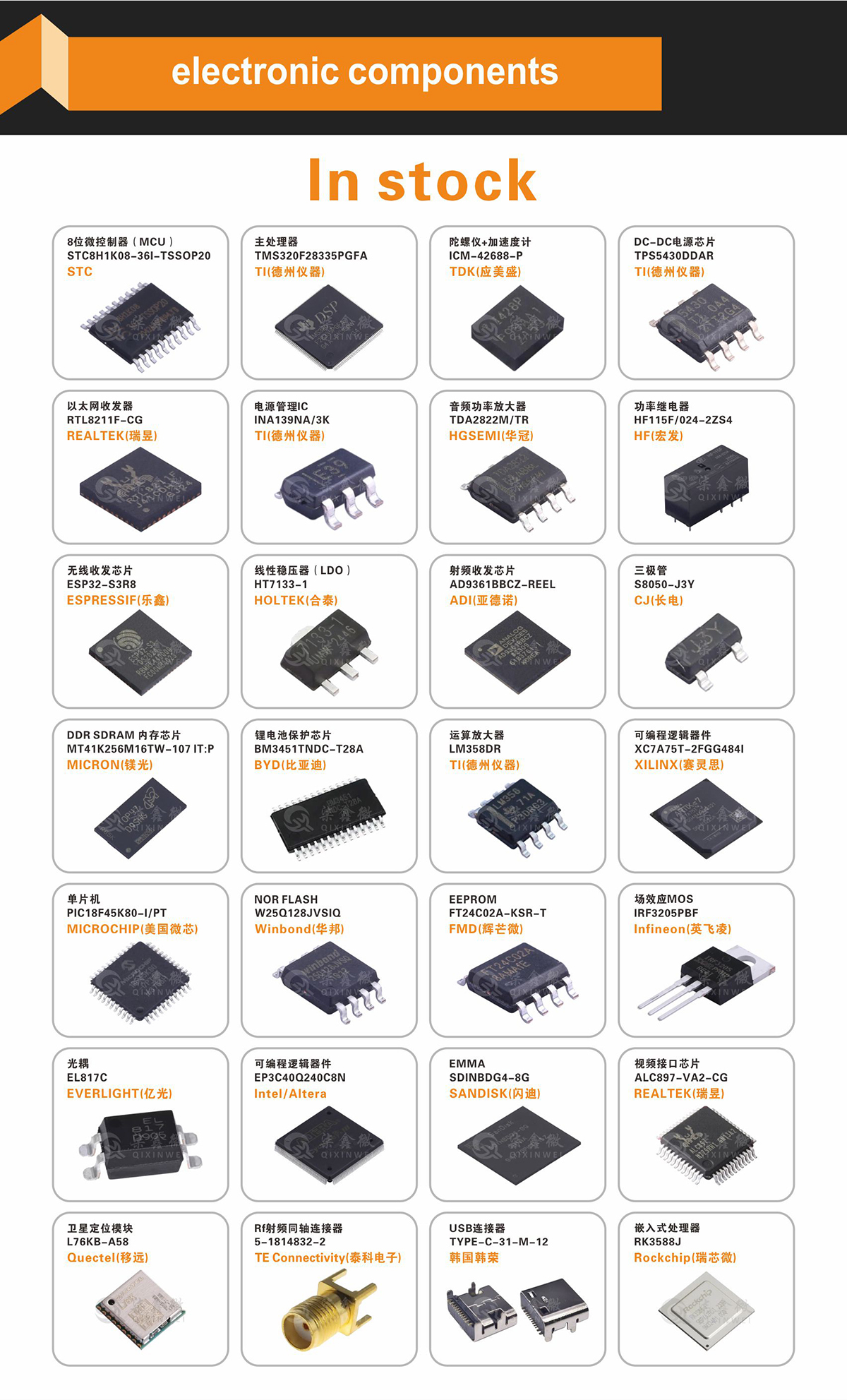
STM32F103VET6 ST Mainstream Arm Cortex-M3 High-Density 32-bit MCU 512KB Flash 72MHz FSMC USB CAN LQFP-100
STM32F103VET6 Product Overview
The STM32F103VET6 is a high-density performance line Cortex-M3 MCU from STMicroelectronics in an LQFP-100 package (14×14×1.4 mm). It features a 72 MHz Cortex-M3 core at 1.25 DMIPS/MHz with single-cycle multiplication and hardware division, 512 KB Flash, and 64 KB SRAM.[reference:30][reference:31] This model is the flagship 100-pin variant in the STM32F103 high-density product line. The MCU integrates FSMC (SRAM/PSRAM/NOR/NAND/Compact Flash), LCD parallel interface, CAN 2.0B, USB 2.0 FS, SDIO, 3×12-bit ADCs (up to 21 channels, 1 µs, triple sample-and-hold), 2×12-bit DACs, 12-channel DMA, up to 11 timers (including 2 advanced-control with PWM/deadtime/emergency stop), and 13 communication interfaces (5×USART/3×SPI/2×I2C/2×I2S/USB/CAN/SDIO). 80 I/Os, all 5 V-tolerant.Supply 2.0–3.6 V, -40–85 °C, ECOPACK®2. Comparison with similar models: Compared to the STM32F103VCT6 (256 KB Flash/48 KB SRAM), both Flash and SRAM are increased. Compared to the STM32F103VBT6 (medium-density, 128 KB Flash/20 KB SRAM), Flash and SRAM are significantly upgraded, and FSMC, SDIO, DAC, a third ADC, more timers, and more communication interfaces are added.
STM32F103VET6 Core Features
Core: Arm Cortex-M3 72 MHz, 1.25 DMIPS/MHz, single-cycle multiplication/hardware division, SWD & JTAG debug Memory: 512 KB Flash, 64 KB SRAM, CRC, 96-bit unique ID FSMC: External SRAM/PSRAM/NOR/NAND/Compact Flash, 4 chip selects; LCD 8080/6800 interface SDIO + CAN + USB: Storage card interface, industrial bus, full-speed USB 3×12-bit ADCs: Up to 21 channels, 1 µs, triple sample-and-hold, temperature sensor 2×12-bit DACs: Buffered output Timers: 2× advanced-control (6-ch PWM/deadtime), 4× GP (quadrature encoder), 2× basic (DAC drive), 2× watchdogs, SysTick Communication Interfaces: 5×USART (ISO7816/LIN/IrDA), 3×SPI (18 Mbit/s), 2×I2C (SMBus), 2×I2S DMA: 12 channels I/Os: 80, all 5 V-tolerant Low Power: Sleep/Stop/Standby, VBAT backup RTC Package: LQFP-100 (14×14×1.4 mm)
STM32F103VET6 Applications
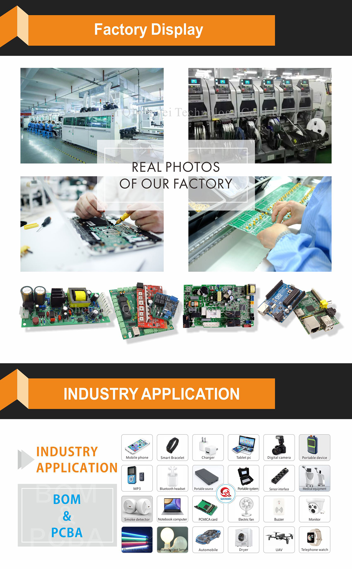
Industrial: PLCs, inverters, CAN nodes, motor drive & control Dual-Motor FOC Control: 2 advanced-control timers Complex Systems: External SRAM/NAND expansion with direct TFT-LCD drive Medical & Handheld Devices IoT Gateways, Smart Home Automotive: Sensor nodes (non-safety-critical) Video Intercom, HVAC, Imaging & Vision
STM32F103VET6 Key Advantages
512 KB Flash + 64 KB SRAM: Flagship configuration in the STM32F103 100-pin family for large firmware and complex algorithms FSMC + LCD Parallel Interface: External memory expansion and direct TFT-LCD drive without an external LCD controller Dual Advanced Timers: Independent dual-motor FOC control 3×12-bit ADCs (21-ch): Triple sample-and-hold for multi-sensor synchronous acquisition 2×12-bit DACs: Buffered output for audio/sensor excitation/control loops Peripheral Superset: SDIO, CAN, USB, 5 USARTs, 3 SPIs, 2 I2S 80 I/Os: LQFP-100 package, extremely rich I/O resources Mature STM32 Ecosystem: CubeIDE/CubeMX/HAL/LL
Why Choose QIXINWEI
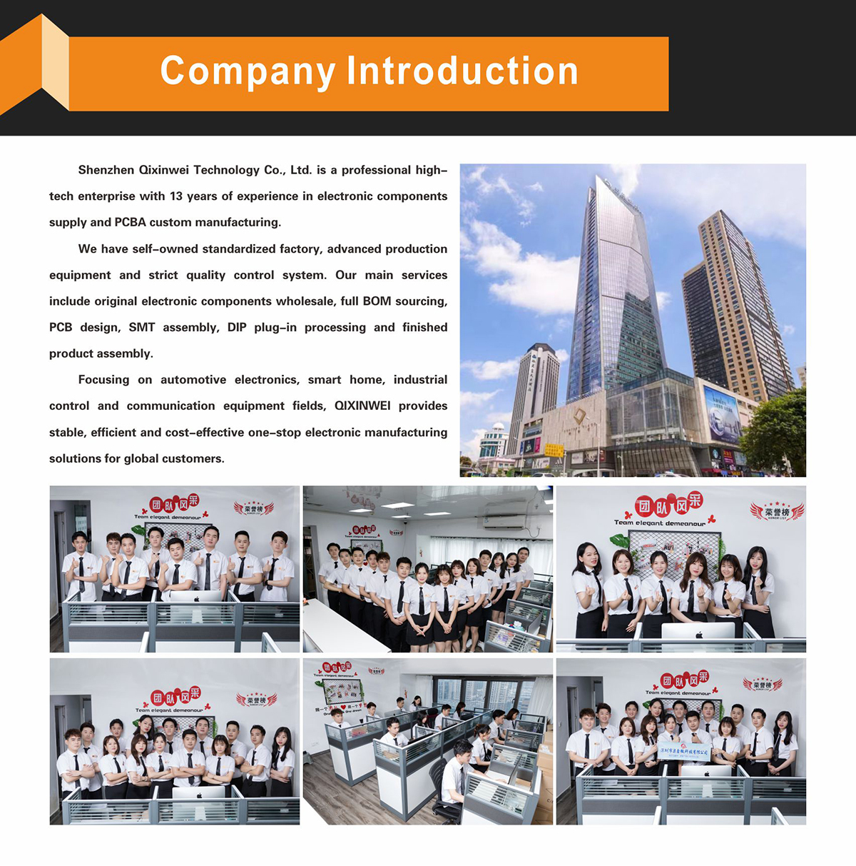
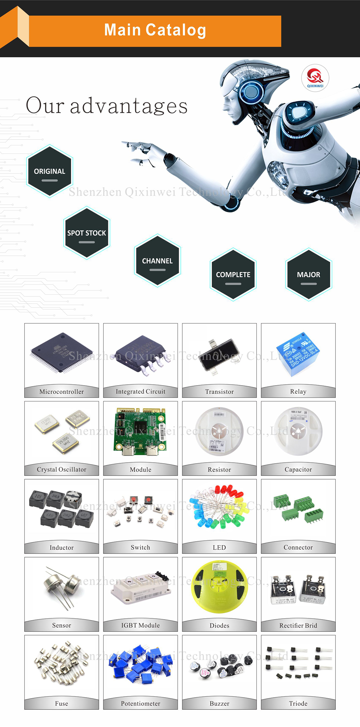
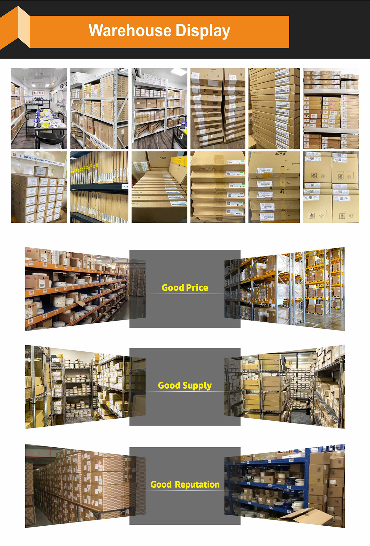
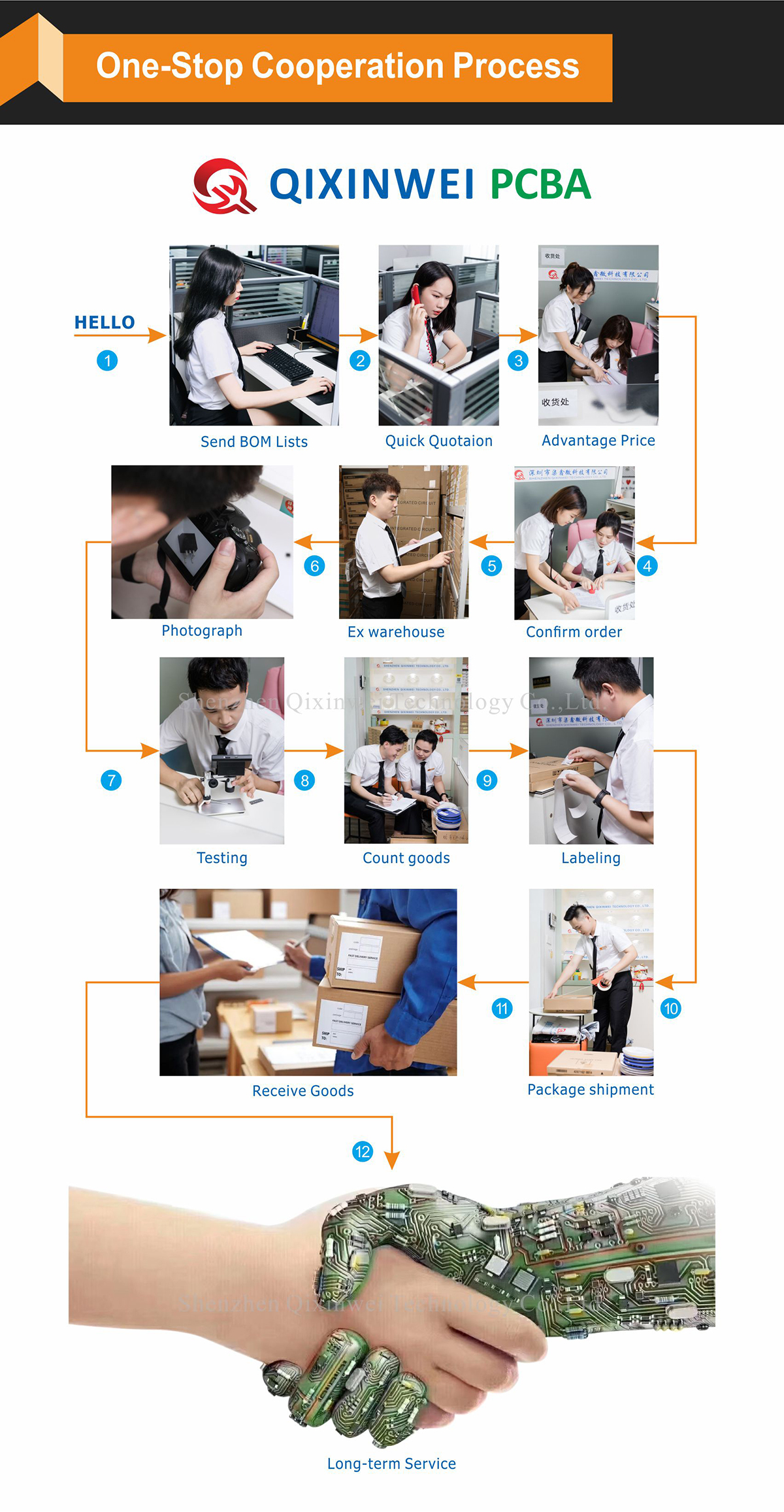
Years of experience in the electronics industry. Trusted by global customers. Massive In-Stock Inventory – Ready to ship promptly BOM Matching Service – One-stop solution, save time PCBA Customization – Professional engineering team creates tailor-made solutions based on your needs Cost-Effective & Efficient – Better channel, better cost A dedicated team makes your procurement smoother. Contact us for BOM quotes or PCBA inquiries.

FAQ:
What is the STM32F103VET6 and why is it one of the most popular F103 variants?
The STM32F103VET6 is a 72 MHz Arm Cortex‑M3 microcontroller with 512 KB Flash, 64 KB SRAM, and an FSMC external memory controller, all in an LQFP‑100 package. It hits the sweet spot between memory capacity, I/O count, and cost, making it the go‑to choice for a vast range of industrial control, motor drive, and consumer applications. Its mature ecosystem and proven reliability have made it a staple in embedded designs for over a decade.How does the STM32F103VET6 differ from the VFT6 and VGT6? When should I choose the VET6?
All three share the same LQFP‑100 package, FSMC, and peripherals. The VET6 provides 512 KB Flash and 64 KB SRAM. The VFT6 increases Flash to 768 KB and SRAM to 96 KB, while the VGT6 offers 1 MB Flash and 96 KB SRAM. Choose the VET6 when your firmware fits comfortably within 512 KB and you want the most cost‑optimized solution. The VFT6 and VGT6 are pin‑compatible upgrades if you later need more code or data space without any PCB changes.Is 512 KB Flash and 64 KB SRAM enough for a complex RTOS, communication stacks, and application logic?
Absolutely. A real‑time operating system, a CANopen or Modbus protocol stack, and a substantial application can easily fit within 512 KB of Flash. The 64 KB SRAM provides sufficient room for communication buffers, task stacks, and real‑time data. Millions of industrial devices—PLCs, motor controllers, and building automation nodes—have shipped with this exact configuration, proving its adequacy for all but the most memory‑hungry tasks.What can I do with the FSMC on the STM32F103VET6? What external memory is supported?
The FSMC (Flexible Static Memory Controller) allows you to connect external parallel NOR Flash, PSRAM, NAND Flash, and even memory‑mapped LCD displays. On the LQFP‑100 package, you can use a 16‑bit data bus to add up to 64 MB of external SRAM or PSRAM for data logging, frame buffers, or additional code storage. Note that the FSMC does not support SDRAM; that requires the STM32F4 series.Can the VET6 replace an older STM32F103VCT6? What benefits do I gain?
Yes, the VET6 is a direct, pin‑compatible upgrade from the VCT6. You double the Flash from 256 KB to 512 KB and increase SRAM from 48 KB to 64 KB without any PCB changes. All peripherals and I/O assignments remain identical, making it the simplest way to extend the life and capability of an existing F103‑based product.How does the STM32F103VET6 compare to the STM32F107? When should I pick one over the other?
The STM32F107 adds an Ethernet MAC and a second CAN to the same Cortex‑M3 core, but keeps the Flash at 256 KB and SRAM at 64 KB. The VET6 removes Ethernet and the second CAN, and in return gives you twice the Flash (512 KB). If your application does not need native Ethernet, the VET6 provides far more code storage headroom. Both are LQFP‑100 and largely pin‑compatible, so migration between them is straightforward.Can the STM32F103VET6 run multiple UART, SPI, I2C, and CAN interfaces simultaneously?
Yes, with up to 82 I/O pins, you can easily accommodate five USART/UART ports, three SPI interfaces, two I2C buses, one CAN 2.0B channel, a USB 2.0 full‑speed device, and still have pins left for the FSMC bus and general‑purpose I/O. STM32CubeMX helps you verify the exact pin‑multiplexing for your configuration.Is the STM32F103VET6 still a good choice for new designs, or should I move to an STM32F2 or F4?
The VET6 remains a solid choice for applications that do not require the higher clock speeds, FPU, or advanced peripherals of the F2/F4 series. Its 512 KB Flash, FSMC, and 100‑pin package are still highly competitive in cost, and the vast ecosystem of libraries, tools, and community knowledge significantly reduces development time and risk. If your design needs Ethernet, a camera interface, or digital signal processing, consider migrating to the F2 or F4. Otherwise, the VET6 provides a reliable, long‑term‑available platform.What low‑power modes does the STM32F103VET6 support, and what is the typical Stop‑mode current?
The chip supports Sleep, Stop, and Standby modes. In Stop mode with the main regulator off and all 64 KB SRAM retained, the typical current is around 14 µA. Wake‑up from Stop is fast enough to respond to external interrupts or communication events. While not as power‑efficient as the STM32L series, it can still be used in battery‑powered devices that spend most of their time in deep sleep.Can I perform over‑the‑air (OTA) firmware updates with the 512 KB single‑bank Flash?
Yes. You can partition the 512 KB Flash into a bootloader, an active application area, and a download buffer. A typical split reserves 16–32 KB for the bootloader, leaving about 480 KB for the application. The 64 KB SRAM can temporarily hold the new firmware image received via USB, UART, or a wireless module. A CRC or signature check ensures a safe update without hardware dual‑bank Flash.
- Product Type:
- Mainstream Arm Cortex-M3 High-Density 32-bit MCU
- Brand:
- STMicroelectronics
- Core:
- Arm Cortex-M3 72MHz
- Package:
- LQFP-100 (14×14×1.4mm)
- Memory:
- 512KB Flash, 64KB SRAM
- Peripherals:
- FSMC, LCD parallel I/F, CAN 2.0B, USB 2.0 FS, SDIO, 3×12-bit ADCs (21ch/1µs), 2×12-bit DACs, 2×16-bit advanced-control timers (PWM/deadtime), 4×16-bit GP timers (quadrature encoder), Calendar RTC, CRC
- Interfaces:
- 2×I2C (SMBus), 3×SPI (18Mbit/s), 2×I2S, 5×USART (ISO7816/LIN/IrDA)
- I/Os:
- 80
- Voltage:
- 2.0V~3.6V
- Temperature:
- -40°C~85°C


