
qixinwei-pcba


STM32F103C8T6 ST Mainstream Arm Cortex-M3 Performance Line 32-bit MCU 64KB Flash 72MHz CPU USB CAN LQFP-48
STM32F103C8T6 Product Overview
The STM32F103C8T6 is a mainstream Arm Cortex-M3 performance line MCU from STMicroelectronics, medium-density product line, LQFP-48 package (7×7 mm). 72 MHz Cortex-M3 core, 1.25 DMIPS/MHz, single-cycle multiplication and hardware division. 64 KB Flash, 20 KB SRAM. This model is one of the highest-volume parts in the STM32F103 family, widely used across embedded systems. It integrates CAN 2.0B, USB 2.0 FS, dual 12-bit ADCs (10 channels, 1 µs), 7-channel DMA, 7 timers (3×16-bit GP/IC/OC/PWM/quadrature encoder, 1×16-bit advanced-control/PWM/deadtime, 2 watchdogs, 24-bit SysTick), 9 communication interfaces (2×I2C/3×USART/2×SPI/USB/CAN). 37 I/Os, all 5 V-tolerant, mappable on 16 external interrupt vectors. VDD 2.0 V–3.6 V, -40 °C to 85 °C, ECOPACK®2. Product Line Positioning: Compared to the STM32F103C6T6/C6T6A (32 KB Flash/10 KB SRAM), this model offers double the Flash and SRAM, plus an advanced-control timer (PWM/deadtime) suitable for motor control and complex industrial applications. Compared to the STM32F103CBT6 (128 KB Flash), this model provides 64 KB Flash at a more cost-effective price point.
STM32F103C8T6 Core Features
Core: Arm Cortex-M3 72 MHz, 1.25 DMIPS/MHz, single-cycle multiplication/hardware division, SWD & JTAG debug, 43 maskable interrupt channels Memory: 64 KB Flash, 20 KB SRAM, CRC, 96-bit unique ID CAN 2.0B: Industrial fieldbus communication USB 2.0 FS: BCD and LPM support Dual 12-bit ADCs: 10 channels, 1 µs, 0–3.6 V, temperature sensor 7-ch DMA: Supporting timers, ADC, SPI, I2C, USART 7 Timers: 3×16-bit GP (IC/OC/PWM/quadrature encoder/pulse counter), 1×16-bit advanced-control (PWM/deadtime/emergency stop), 2 watchdogs, 24-bit SysTick Communication: 2×I2C (SMBus/PMBus), 3×USART (ISO 7816/LIN/IrDA/modem control), 2×SPI (18 Mbit/s), USB 2.0 FS, CAN 2.0B Low Power: Sleep/Stop/Standby, VBAT for RTC and backup registers Clock: 4–16 MHz XTAL, 32 kHz RTC XTAL (calibrated), 8 MHz RC (factory-trimmed), 40 kHz RC, PLL I/Os: 37 fast I/Os, all 5 V-tolerant, mappable on 16 ext. interrupt vectors Supply/Temp: VDD 2.0 V–3.6 V, POR/PDR/PVD, -40 °C to 85 °C Package: LQFP-48 (7×7×1.4 mm), Tray
STM32F103C8T6 Applications
Industrial: PLCs, sensor transmitters, RS-485/CAN nodes, inverters Motor Control: BLDC motors, servo motors, fans, pumps (advanced-control timer with 6-ch PWM/deadtime/emergency stop) Consumer: Remote controls, handhelds, PC peripherals, GPS platforms, gaming peripherals Medical: Handheld medical terminals, health monitoring devices Home Appliances: Panels, HVAC, alarms, video intercoms Security: Access control, alarms, smoke detectors IoT: Wireless sensors, environmental monitoring, smart home LED Lighting: Dimming, RGB strips, SMPS Automotive: Light control, window anti-pinch, sensor nodes (non-safety-critical)
STM32F103C8T6 Key Advantages
Arm Cortex-M3 Core: 72 MHz, 1.25 DMIPS/MHz, single-cycle multiplication/hardware division, far exceeding Cortex-M0/M0+ performance CAN + USB Dual Interface: Rare in this class, meeting both industrial bus and general communication needs 64 KB Flash + 20 KB SRAM: For medium-to-high complexity applications 7 Timers (incl. Advanced-Control): 1 advanced-control timer (6-ch PWM/deadtime/emergency stop) + 3 GP timers (quadrature encoder), ideal for motor control and complex timing generation Dual 12-bit ADCs: 1 µs conversion time, 10 channels, temperature sensor, separate analog supply LQFP-48 Package: 7×7 mm, 37 I/Os (all 5 V-tolerant), balanced package size and I/O resources 7-ch DMA: Direct peripheral-to-memory transfers, offloads CPU 9 Communication Interfaces: 2×I2C + 3×USART + 2×SPI + USB + CAN, meeting multi-bus connectivity needs Calendar RTC: VBAT backup, ideal for scheduled sensing and low-power applications Mature STM32 Ecosystem: CubeIDE/CubeMX/HAL/LL libraries, abundant development boards and reference designs (e.g., Blue Pill development board) Cost-Effective Performance Line: 32-bit ARM + CAN + USB + dual ADCs + advanced timer + DMA, ideal upgrade from 8/16-bit MCUs
Why Choose QIXINWEI
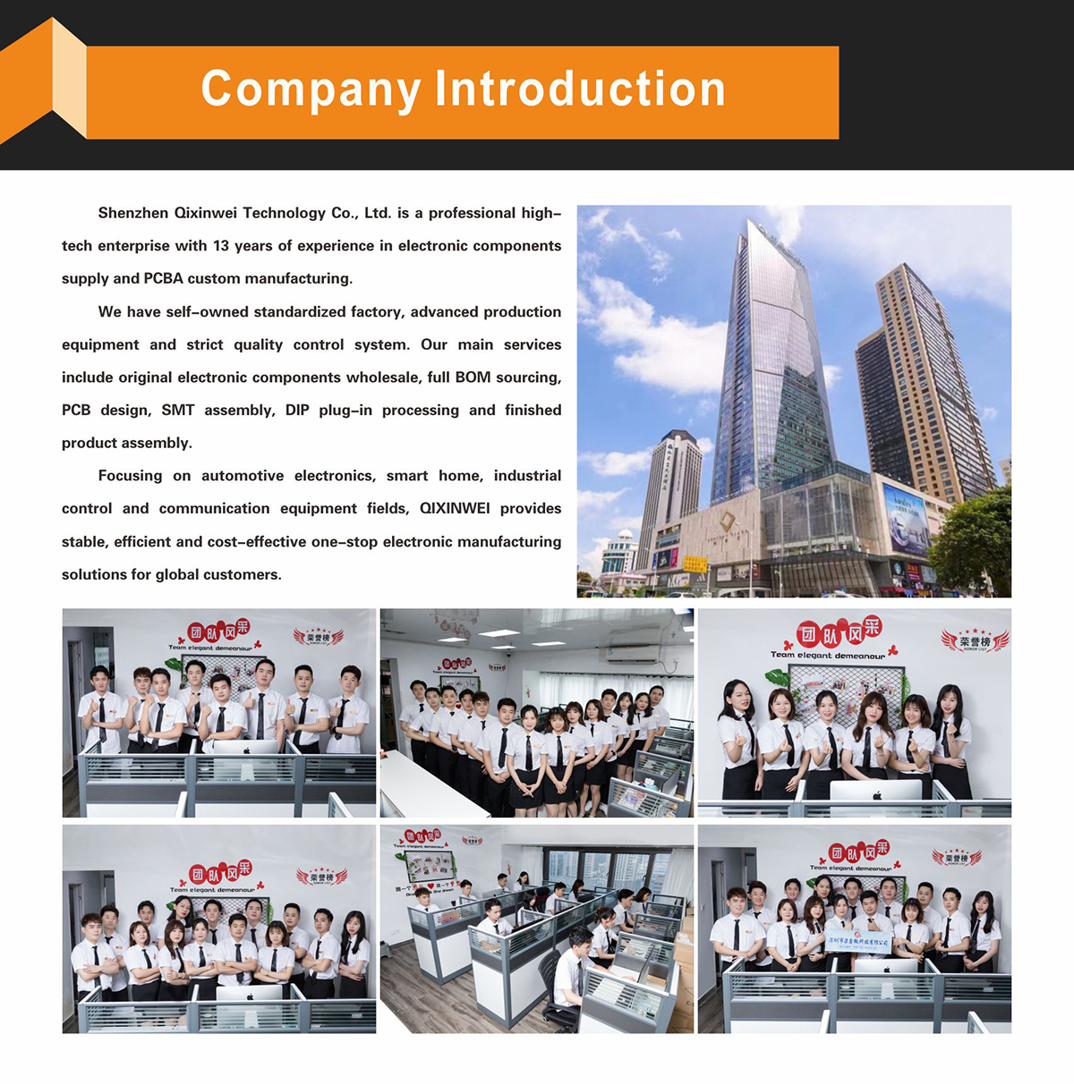
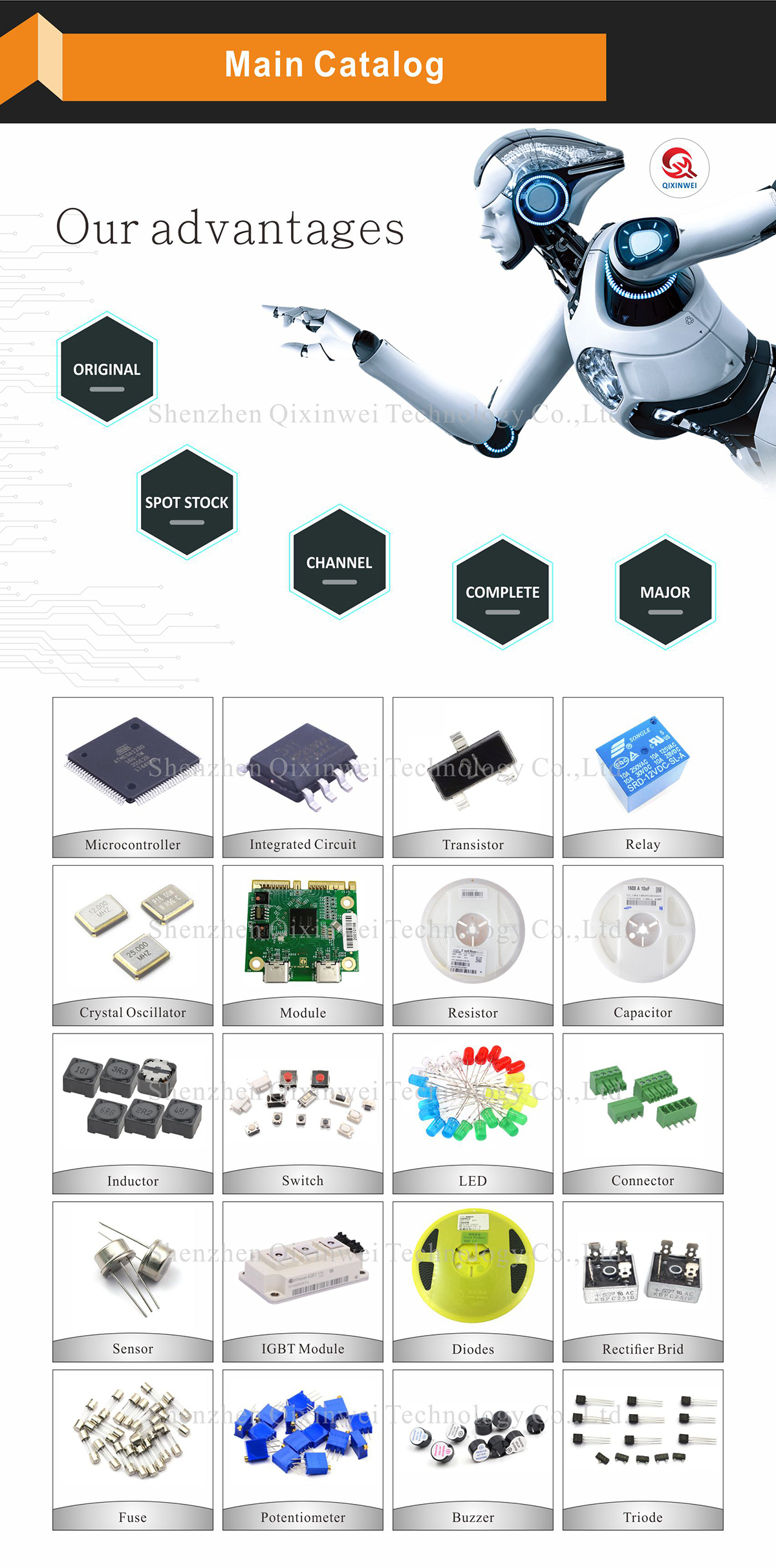
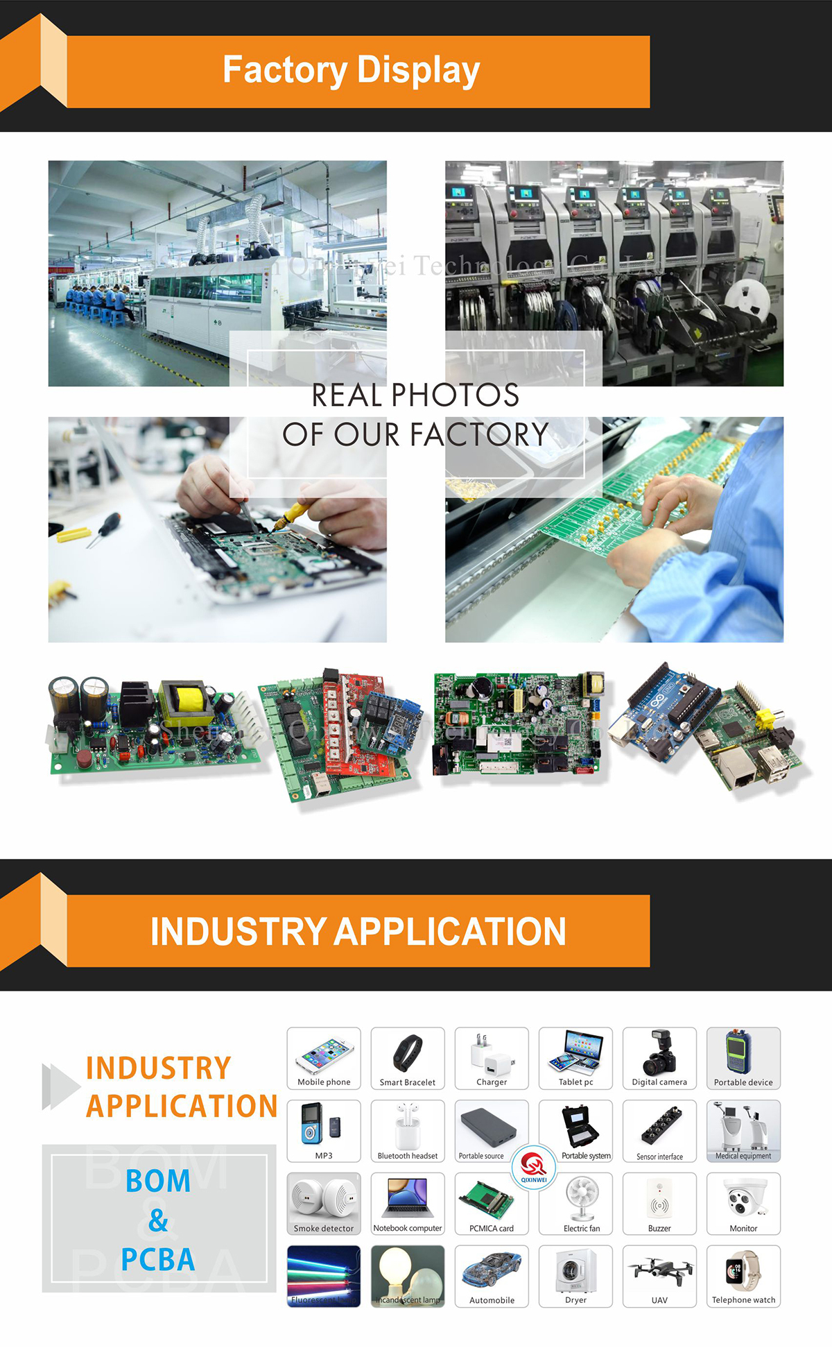
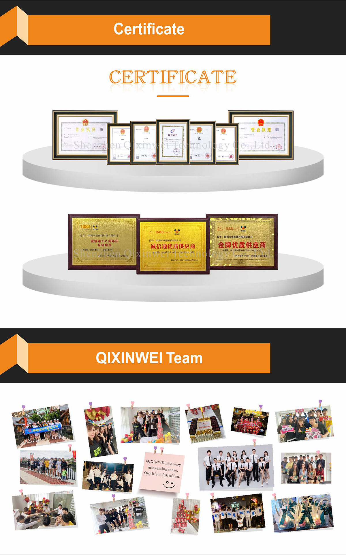
Years of experience in the electronics industry. Trusted by global customers. Massive In-Stock Inventory – Ready to ship promptly BOM Matching Service – One-stop solution, save time PCBA Customization – Professional engineering team creates tailor-made solutions based on your needs Cost-Effective & Efficient – Better channel, better cost A dedicated team makes your procurement smoother. Contact us for BOM quotes or PCBA inquiries.




FAQ:
What is the STM32F103C8T6 and why is it so popular?
The STM32F103C8T6 is a 72 MHz Arm Cortex‑M3 microcontroller with 64 KB Flash and 20 KB SRAM, housed in an LQFP‑48 package. It is the most widely recognized member of the STM32F103 family, often referred to as the "Blue Pill" chip. Its combination of a proven 32‑bit core, essential peripherals (CAN, USB, multiple USART/SPI/I2C), extremely low cost, and massive community support has made it a staple in hobbyist projects, educational platforms, and cost‑sensitive commercial products for over a decade.How does the STM32F103C8T6 differ from the STM32F103CBT6? When should I pick the C8T6?
Both share the same LQFP‑48 package, core, SRAM, and peripherals. The only difference is Flash size: the C8T6 offers 64 KB, while the CBT6 provides 128 KB. Choose the C8T6 when your firmware fits comfortably within 64 KB and you want the absolute minimum cost entry point into the STM32F1 ecosystem. The pin‑compatible CBT6 is a direct drop‑in upgrade if you later need double the Flash with zero PCB changes.Is 64 KB Flash and 20 KB SRAM really enough for a real‑time control application with CAN and USB?
Absolutely, for dedicated and tightly optimized projects. A bare‑metal CANopen stack, a USB device library, and control logic can be squeezed into 64 KB of Flash. The 20 KB SRAM requires disciplined buffer management—using DMA for serial transfers, placing constants in Flash, and avoiding large static arrays—but countless proven CAN‑to‑USB converters, simple motor controllers, and sensor nodes run comfortably in this space. If your firmware later outgrows the 64 KB limit, the pin‑compatible CBT6 (128 KB Flash) provides a direct upgrade with zero hardware changes.How does the STM32F103C8T6 compare to the STM32F103R8T6? When should I pick the 48‑pin version?
Both share the same 64 KB Flash and 20 KB SRAM. The R8T6 is an LQFP‑64 package with up to 51 I/Os, while the C8T6 uses an LQFP‑48 with up to 37 I/Os. Choose the C8T6 when board space is tight and 37 I/Os are sufficient. The R8T6 provides extra I/Os for designs that need more serial ports or GPIOs without pin conflicts. Both lack the FSMC external memory controller, so the pin‑count difference is the primary deciding factor.Why doesn't the STM32F103C8T6 have an FSMC? How can I add external memory?
The STM32F103C8T6 does not include the FSMC peripheral, which is available only on higher‑end 100‑pin and 144‑pin F103 variants (e.g., VCT6, ZET6). You cannot connect parallel NOR Flash, PSRAM, or NAND Flash. For additional storage, you can use the SPI ports to connect serial Flash (for data or code) or serial SRAM/PSRAM. The internal 64 KB Flash is typically sufficient for compact applications. If your design absolutely requires parallel external memory, you must move to a larger package with FSMC.Can the C8T6 run CAN, USB, and multiple UART/SPI/I2C interfaces simultaneously on its 48‑pin package?
Yes, with careful pin planning. With up to 37 I/Os, you can easily accommodate one CAN 2.0B, one USB 2.0 full‑speed device, two USARTs, one SPI, one I2C, and still have a few GPIOs left. STM32CubeMX helps you verify the exact pin‑multiplexing for your configuration. This makes the C8T6 a capable, compact communication node for industrial gateways and protocol converters.What low‑power modes does the STM32F103C8T6 support, and is it suitable for battery‑powered devices?
The chip supports Sleep, Stop, and Standby modes. In Stop mode with the main regulator off and all 20 KB SRAM retained, the typical current is around 14 µA. Wake‑up from Stop is fast enough to respond to CAN, USB, or external interrupts. While it is not as power‑efficient as the STM32L series, the C8T6 can still be used in battery‑powered sensors and portable instruments that spend most of their time in deep sleep and wake up periodically.Can I perform over‑the‑air (OTA) firmware updates with the 64 KB single‑bank Flash?
Yes. You can partition the 64 KB Flash into a very small bootloader (4–8 KB) and a compact application. The 20 KB SRAM can temporarily buffer the new firmware image received via USB, CAN, UART, or a wireless module. A CRC check ensures a safe update. An A/B update scheme is not practical with this Flash size; a download‑and‑overwrite approach is recommended.Is the STM32F103C8T6 still a good choice for new designs, or should I move to a newer series?
The C8T6 remains a solid choice for cost‑sensitive applications that do not require larger memory, an FSMC, or advanced features of newer series. Its low cost, proven reliability, and mature ecosystem make it ideal for high‑volume products. If your application requires more Flash, SRAM, or FSMC, the pin‑compatible CBT6 or larger 64‑pin RCT6/RET6 are natural upgrades. For Ethernet, advanced security, or ultra‑low power, consider the STM32F2, F4, or L4 series.What development tools and libraries support the STM32F103C8T6? Is the F1 ecosystem mature?
The C8T6 is fully supported by STM32CubeIDE, Keil MDK, and IAR EWARM. The vast STM32F1 HAL/LL library, countless online tutorials, and community‑driven code examples make development straightforward. You can prototype on a NUCLEO‑F103RB board (64‑pin, same core and memory) and then easily migrate to the C8T6 by adjusting the pin‑out and linker script in CubeMX. The "Blue Pill" board specifically has become a de‑facto standard in the maker community, with endless project examples available.
- Product Type:
- Mainstream Arm Cortex-M3 Performance Line 32-bit MCU
- Brand:
- STMicroelectronics
- Core:
- Arm Cortex-M3 72MHz
- Package:
- LQFP-48 (7×7×1.4mm)
- Memory:
- 64KB Flash, 20KB SRAM
- Peripherals:
- CAN 2.0B, USB 2.0 FS, Dual 12-bit ADCs (10ch/1µs), 1×16-bit advanced-control timer (6ch PWM/deadtime), 3×16-bit GP timers (quadrature encoder), Calendar RTC, CRC
- Interfaces:
- 2×I2C (SMBus/PMBus), 3×USART (ISO 7816/LIN/IrDA), 2×SPI (18 Mbit/s)
- I/Os:
- 37
- Voltage:
- VDD 2.0V~3.6V
- Temperature:
- -40°C~85°C


