
qixinwei-pcba


STM32F031G6U6 ST Mainstream Arm Cortex-M0 Access Line 32-bit MCU 32KB Flash 48MHz CPU 12-bit ADC UFQFPN-28
STM32F031G6U6 Product Overview
The STM32F031G6U6 is a mainstream Arm Cortex-M0 access line 32-bit MCU from STMicroelectronics, housed in an ultra-compact UFQFPN-28 package (4×4×0.55 mm). It incorporates a 48 MHz high-performance Arm Cortex-M0 32-bit RISC core, with 32 KB Flash, 4 KB SRAM with hardware parity, and a CRC calculation unit. On-chip peripherals include a 12-bit ADC (up to 10 channels, 1.0 µs conversion time, 13 ADC inputs including external + internal channels), 5-channel DMA controller, calendar RTC with alarm and periodic wakeup and V_BAT backup supply, up to 9 timers (including one 16-bit 7-channel advanced-control timer for 6-channel PWM output with deadtime generation and emergency stop, one 32-bit and three 16-bit general-purpose timers, independent and system window watchdog timers, and SysTick timer), and I2C (Fast Mode Plus 1 Mbit/s), SPI (18 Mbit/s, with I2S interface multiplexed), and USART (supporting master synchronous SPI and modem control, ISO7816 interface, LIN, IrDA, auto baud rate detection and wakeup). The device provides 23 fast I/Os, all mappable on external interrupt vectors. It operates from 2.0 V to 3.6 V over -40 °C to 85 °C (extended temperature range -40 °C to +105 °C optional). All packages are ECOPACK®2 compliant.
STM32F031G6U6 Core Features
Arm Cortex-M0 Core: 32-bit Arm Cortex-M0 RISC core, up to 48 MHz, with built-in Nested Vectored Interrupt Controller Memory: 32 KB Flash, 4 KB SRAM with hardware parity, CRC calculation unit 12-bit ADC: 1.0 µs conversion time, up to 10 channels (13 ADC inputs including external + internal channels), conversion range 0 to 3.6 V, separate analog supply 2.4 V to 3.6 V 5-Channel DMA Controller: Flexible mapping for memory-to-memory, peripheral-to-memory, and memory-to-peripheral transfers 9 Timers: One 16-bit 7-channel advanced-control timer (6-channel PWM output, deadtime generation, emergency stop), one 32-bit general-purpose timer (up to 4 IC/OC, usable for IR control decoding), one 16-bit general-purpose timer (2 IC/OC, supports deadtime generation and emergency stop), one 16-bit general-purpose timer (supports modulator gate for IR control), one 16-bit general-purpose timer (1 IC/OC), independent watchdog, system window watchdog, SysTick timer Calendar RTC: With alarm and periodic wakeup from Stop/Standby, V_BAT backup supply Communication Interfaces: One I2C (Fast Mode Plus 1 Mbit/s, SMBus/PMBus, 20 mA current sink, wakeup from Stop), one USART (supporting master synchronous SPI and modem control, ISO7816 interface, LIN, IrDA, auto baud rate detection and wakeup), one SPI (18 Mbit/s, 4 to 16 programmable bit frames, I2S interface multiplexed) Low-Power Modes: Sleep, Stop, Standby Clock Management: 4–32 MHz crystal oscillator, 32 kHz RTC crystal oscillator with calibration, internal 8 MHz RC with x6 PLL option, internal 40 kHz RC oscillator I/O Resources: 23 fast I/Os, all mappable on external interrupt vectors High Reliability: Power-on/power-down reset (POR/PDR), programmable voltage detector (PVD), serial wire debug (SWD), 96-bit unique ID Wide Operating Range: 2.0 V to 3.6 V, -40 °C to 85 °C (extended temperature range -40 °C to +105 °C optional) Green Packaging: ECOPACK®2 compliant, UFQFPN-28 package (4×4×0.55 mm, 0.5 mm pitch)
STM32F031G6U6 Applications
Consumer Electronics: Remote controls, electric toothbrushes, electronic toys, handheld devices, PC peripherals (printers, scanners) Industrial Control: Sensor transmitters, RS-485 communication nodes, small actuators, process monitoring Home Appliances: Induction/microwave oven panels, HVAC systems, alarm systems, smart lighting IoT Nodes: Wireless sensor terminals, environmental monitoring modules, smart home control LED Lighting: Dimming control, RGB strip drivers, switching power supply management Motor Control: Fans, pumps, small motor drives — advanced-control timer supports 6-channel PWM output, deadtime generation, and emergency stop Automotive Electronics: Vehicle light control, window anti-pinch, automotive sensor nodes (non-safety-critical)
STM32F031G6U6 Key Advantages
Arm Cortex-M0 32-bit Performance: 48 MHz high-performance 32-bit ARM core, far exceeding 8/16-bit MCU processing capability for complex algorithms UFQFPN-28 Ultra-Compact Package: 4×4 mm compact footprint, 0.5 mm pin pitch, 23 fast I/Os, ideal for space-constrained applications 32 KB Flash + 4 KB SRAM Configuration: 32 KB Flash program memory, 4 KB SRAM with hardware parity, meeting storage needs for low-to-medium complexity applications 12-bit High-Speed ADC: 1.0 µs conversion time, up to 10 channels (13 ADC inputs), separate analog supply, analog watchdog for precise monitoring 5-Channel DMA Offloads CPU: Enables direct data transfer between peripherals and memory, significantly reducing CPU load I2C Fast Mode Plus: 1 Mbit/s communication rate, 20 mA high current sink capability, SMBus/PMBus support — ideal for power management and sensor applications Rich Timer Resources: One 16-bit 7-channel advanced-control timer (6-channel PWM, deadtime generation, emergency stop) + one 32-bit general-purpose timer (supporting IR control decoding) — ideal for motor control and infrared remote control applications SPI with I2S Multiplexing: SPI interface supports 18 Mbit/s communication rate with I2S audio interface multiplexed for audio applications Calendar RTC: Built-in hardware RTC with alarm and periodic wakeup, V_BAT backup supply — ideal for scheduled sensing and low-power applications Mature STM32 Ecosystem: Compatible with STM32CubeIDE, STM32CubeMX, HAL libraries, abundant development boards and reference designs Cost-Effective Access Line: 32-bit ARM performance at a competitive price — the ideal upgrade path from 8/16-bit MCUs
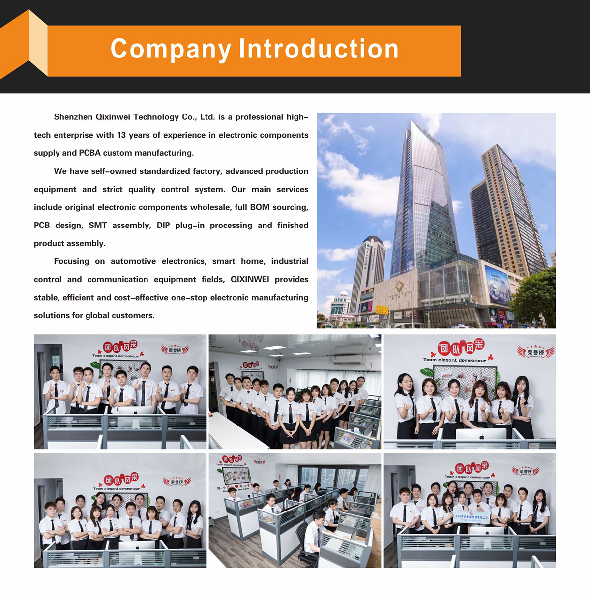
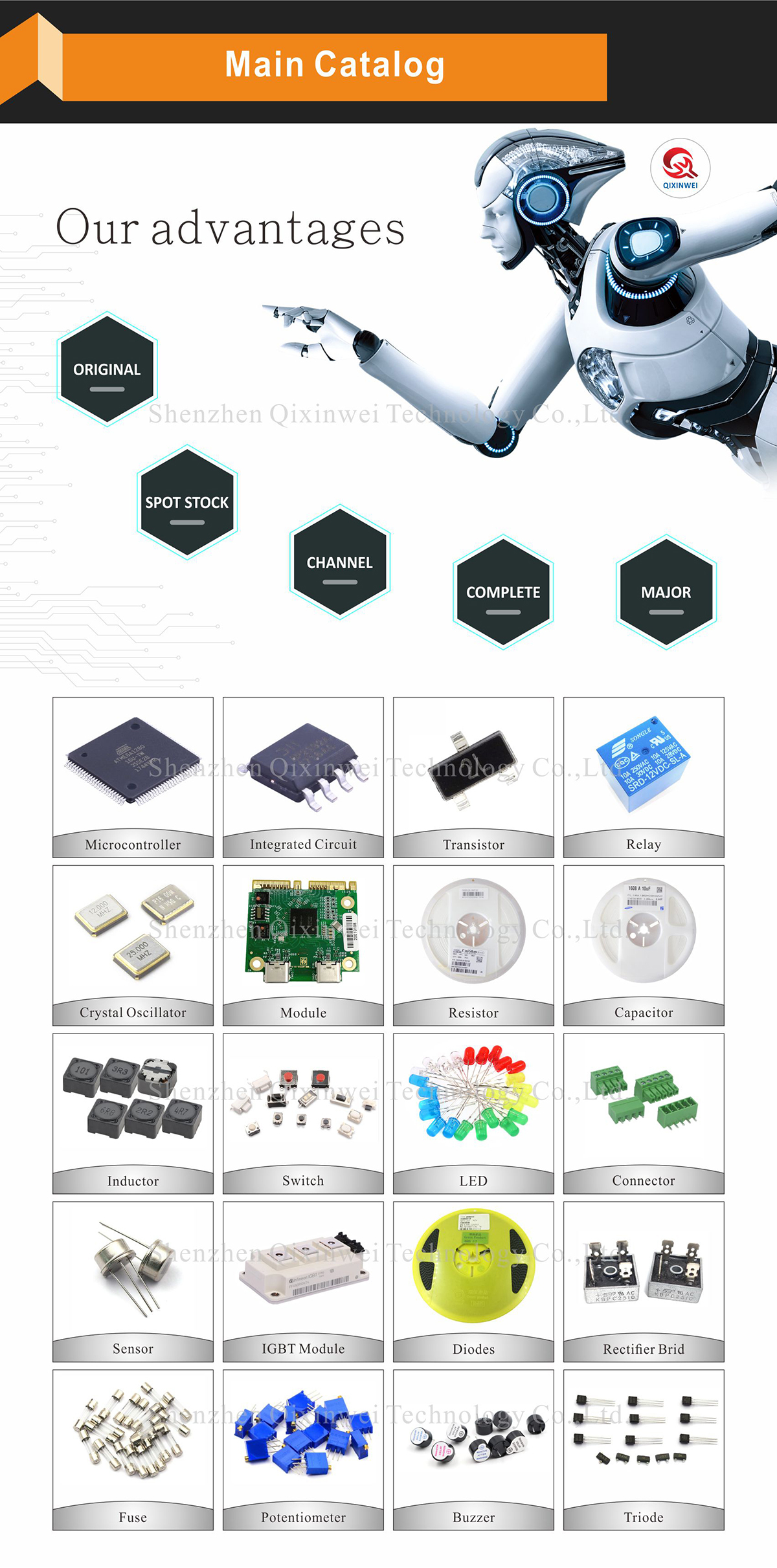
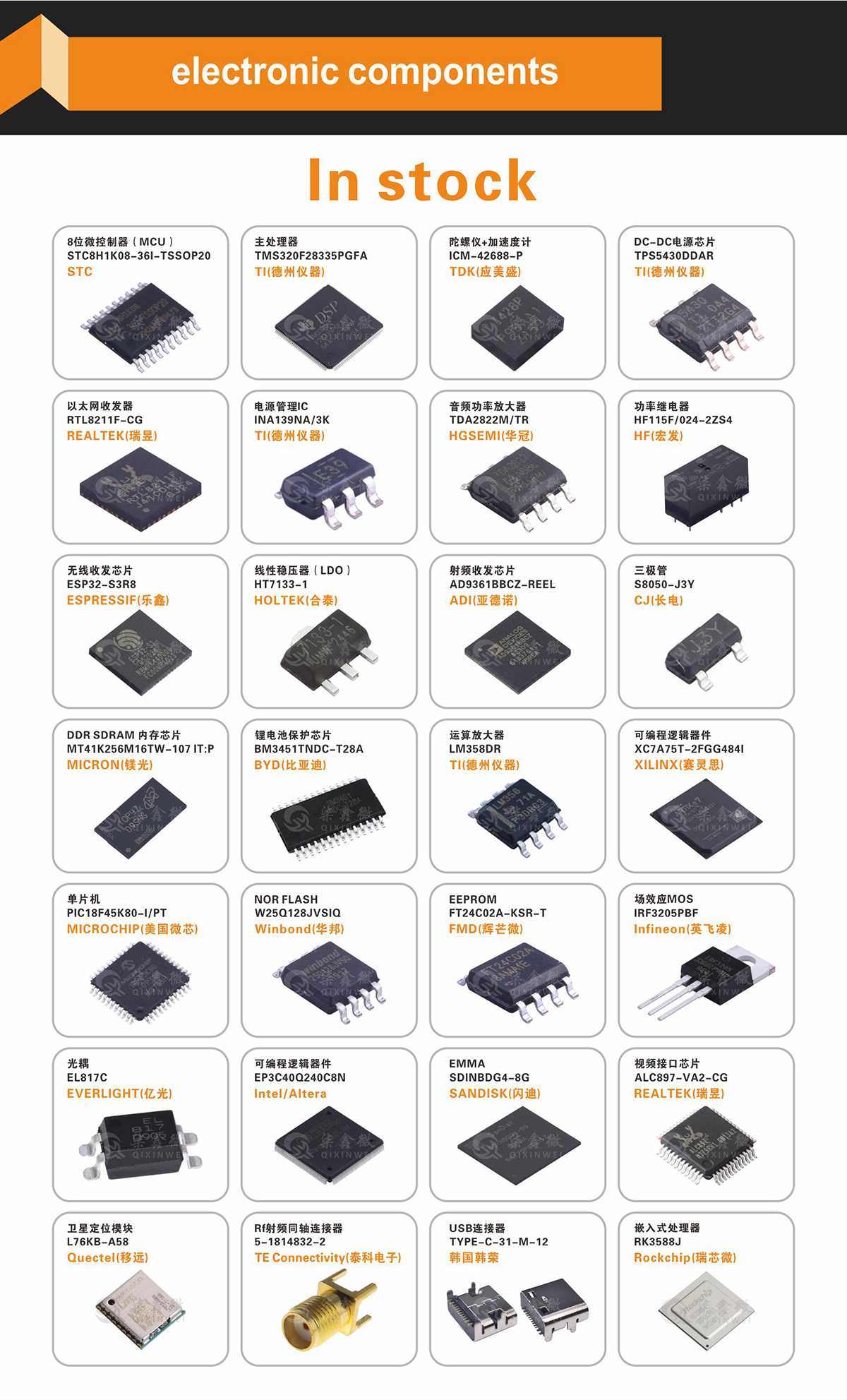
Why Choose QIXINWEI
Years of experience in the electronics industry. Trusted by global customers.
Massive In-Stock Inventory – Ready to ship promptly
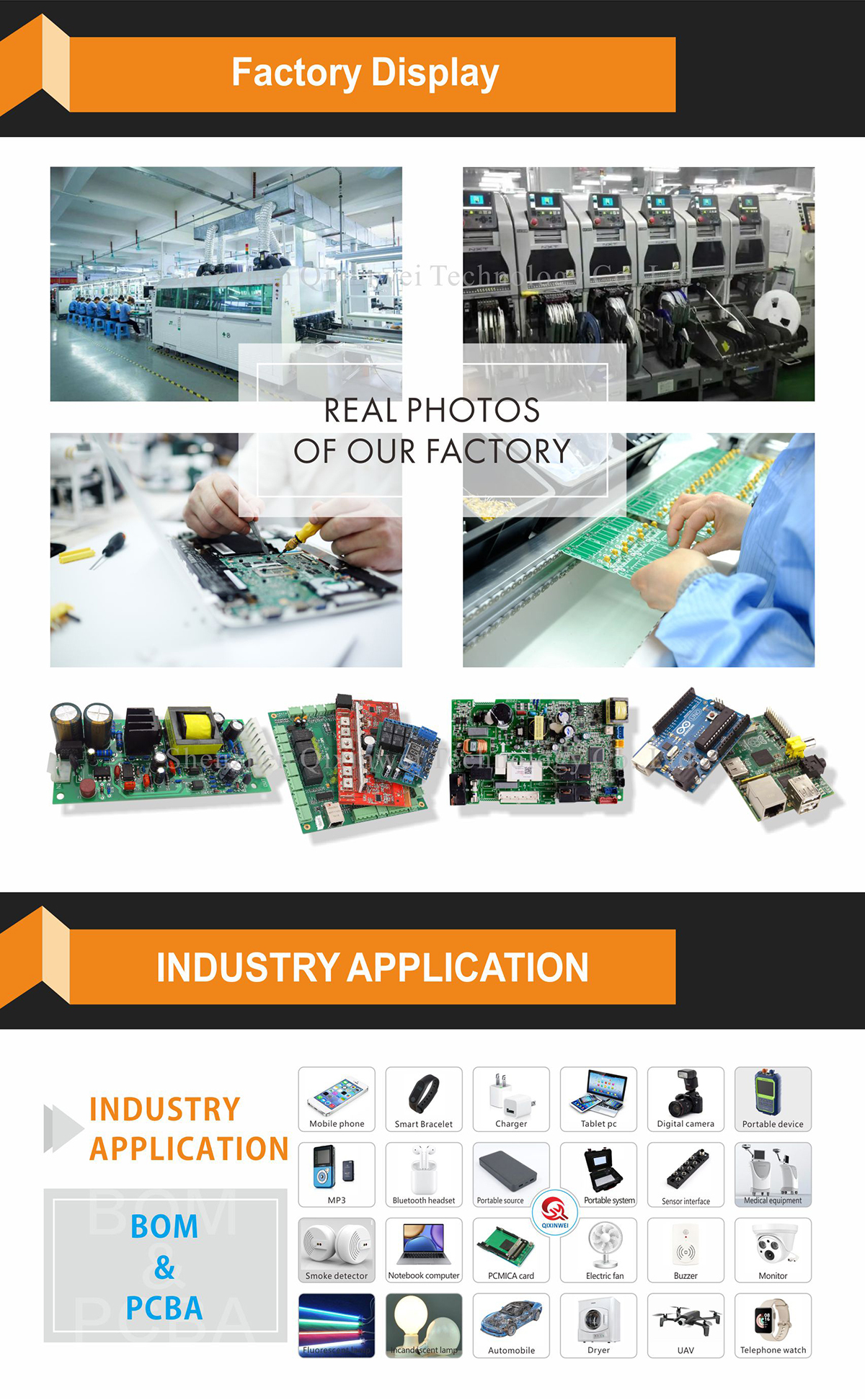
BOM Matching Service – One-stop solution, save time
PCBA Customization – Professional engineering team creates tailor-made solutions based on your needs
Cost-Effective & Efficient – Better channel, better cost
A dedicated team makes your procurement smoother.
Contact us for BOM quotes or PCBA inquiries





FAQ:
What is the STM32F031G6U6 and what are its key specifications?
The STM32F031G6U6 is a 32‑bit ARM Cortex‑M0 microcontroller from STMicroelectronics, running at up to 48 MHz with 32 KB of Flash memory and 4 KB of SRAM. It integrates a 12‑bit 1 Msps ADC, an advanced‑control timer (TIM1) capable of generating four complementary PWM outputs with hardware dead‑time insertion, and standard serial interfaces including USART, SPI, and I2C. All of this is packed into an ultra‑small 4×4 mm UFQFPN28 package, making it ideal for space‑constrained, cost‑sensitive applications such as sensor nodes, portable medical devices, power tools, and compact brushless motor drivers.What are the package dimensions and pin pitch of the STM32F031G6U6?
It uses a UFQFPN28 package that measures only 4 mm × 4 mm with a thickness of 0.55 mm and a lead pitch of 0.5 mm. The package features an exposed bottom pad that enhances thermal dissipation and provides a solid ground connection. This tiny footprint is perfect for high‑density, ultra‑compact PCB designs, and the 0.5 mm pitch is well within the capabilities of modern SMT assembly processes.How does the STM32F031G6U6 differ from the STM32F030G6U6, and how should I choose between them?
Both devices are nearly pin‑compatible and share the same 48 MHz Cortex‑M0 core, 32 KB Flash, and 4 KB SRAM in a UFQFPN28 package. The critical difference is in the timer peripherals: the STM32F031G6U6 adds an advanced‑control timer (TIM1) that provides up to four complementary PWM pairs with programmable dead‑time and a break input, making it directly suitable for driving brushless DC motors or half‑bridge power stages. The STM32F030G6U6 offers only basic timers like TIM3 and TIM14. Choose the F031G6 if your application requires motor control or synchronous rectification; opt for the F030G6 for simpler timing needs where cost may be slightly lower.How does the STM32F031G6U6 compare with the STM32F042F6P6? Which one should I pick for a tiny project?
Both are Cortex‑M0 MCUs clocked at 48 MHz, but they target different requirements. The STM32F042F6P6, available in TSSOP‑20 or UFQFPN‑28, includes a USB 2.0 full‑speed device controller and a CAN 2.0B interface, while its timers are basic. The STM32F031G6U6 omits USB and CAN to focus on the advanced motor‑control timer TIM1 and a 12‑bit 1 Msps ADC, all in a smaller 4×4 mm package. Pick the F042F6P6 if you need USB or CAN communication; choose the F031G6U6 when you need compact motor drive capability or high‑performance analog sensing without the extra communication peripherals.Is 32 KB Flash and 4 KB SRAM really enough for motor control algorithms and communication stacks?
Yes, with disciplined firmware optimization. 32 KB of Flash can comfortably hold a field‑oriented control (FOC) or six‑step commutation algorithm, a USART/SPI communication stack, and sensor drivers, often with room left for future updates. The 4 KB SRAM requires careful management—keeping lookup tables and constants in Flash and using DMA for ADC and serial transfers minimizes RAM consumption. Numerous proven designs in power tools, drone ESCs, and industrial actuators demonstrate reliable operation within these limits. If your firmware later outgrows the 4 KB SRAM, you can migrate to the STM32F071C8T6 (64 KB Flash, 16 KB SRAM) or the STM32G0 series.What are the ADC specifications for the STM32F031G6U6, and how many analog channels are available?
It contains a single 12‑bit successive‑approximation ADC with a maximum sampling rate of 1 Msps. Although the ADC module internally supports up to 13 external channels, the 28‑pin UFQFPN package exposes 10 of them (IN0–IN9) through pins PA0–PA7 and PB0–PB1. Internal channels for the temperature sensor and the voltage reference are also available. This high‑speed, multi‑channel ADC makes the chip well‑suited for multi‑sensor data acquisition, such as phase‑current sensing in sensorless motor control or environmental monitoring nodes.Can the STM32F031G6U6 be powered by 5 V? Are its GPIO pins 5‑volt tolerant?
The chip must be powered with a supply voltage between 2.0 V and 3.6 V; applying 5 V directly to the VDD pin is not allowed. However, most I/O pins (including PA0–PA7, PB0–PB1, PF0–PF1) are marked as FT (5‑volt tolerant) and can safely withstand input voltages up to 5 V. This allows you to directly interface with 5 V logic devices—either by reading their outputs or by using an open‑drain configuration with a pull‑up resistor—without needing external level shifters, significantly simplifying mixed‑voltage designs.How low is the power consumption of the STM32F031G6U6, and is it suitable for battery‑operated devices?
The chip features excellent low‑power performance. In Run mode at 48 MHz with all peripherals enabled, the typical current is around 12.3 mA. Sleep mode reduces this to approximately 2.5 mA. In Stop mode, with all 4 KB of SRAM and registers retained, the current drops to about 5 µA; Standby mode reduces it further to around 1.2 µA. Wake‑up from Stop mode is fast enough to respond to external interrupts or incoming UART data. These characteristics make the STM32F031G6U6 extremely well‑suited for battery‑powered or energy‑harvesting applications where the system sleeps most of the time and wakes periodically to perform short tasks.How do I program and debug the STM32F031G6U6? What development tools are needed?
Programming and debugging are performed via the SWD (Serial Wire Debug) interface, requiring only the SWDIO, SWCLK, VCC, and GND connections. A low‑cost ST‑LINK/V2 or STLINK‑V3 debugger is all you need. For software, STMicroelectronics provides the completely free STM32CubeIDE, and the chip is also supported by Keil MDK and IAR EWARM. Using STM32CubeMX for graphical pinout and peripheral configuration dramatically speeds up the initial setup. Comprehensive HAL and LL libraries along with numerous example projects are available, enabling a very quick start to prototyping and production development.What are the most typical applications for the STM32F031G6U6?
It excels in compact brushless DC motor drives (power tools, drone ESCs, micro pumps), sensor‑intensive industrial nodes, portable medical instruments, battery chargers, and cost‑effective smart actuators. Any space‑constrained embedded system that needs a 12‑bit 1 Msps ADC, advanced motor‑control PWM (TIM1), and a 32‑bit Cortex‑M0 core in a tiny 4×4 mm package is a strong match for the F031G6U6. Its mature STM32F0 ecosystem and very low operating power make it equally popular for mass production and rapid prototyping.
- Product Type:
- Mainstream Arm Cortex-M0 Access Line 32-bit MCU
- Brand:
- STMicroelectronics
- Core:
- Arm Cortex-M0 48MHz
- Package:
- UFQFPN-28 (4×4×0.55mm)
- Memory:
- 32KB Flash, 4KB SRAM (with hardware parity)
- Peripherals:
- 12-bit ADC (10ch/1.0µs/13 ADC inputs), 16-bit 7ch advanced-control timer (6-ch PWM), 32-bit GP timer, 3x 16-bit GP timers, Calendar RTC, CRC
- Interfaces:
- I2C (Fast Mode Plus), SPI (18 Mbit/s, I2S mux), USART (ISO7816/LIN/IrDA)
- I/Os:
- 23
- Voltage:
- 2.0V~3.6V
- Temperature:
- -40°C~85°C


