
qixinwei-pcba


STM32C031F6P6 ST Mainstream Arm Cortex-M0+ 32-bit MCU 32KB Flash 48MHz CPU 12-bit ADC TSSOP-20
STM32C031F6P6 Product Overview
The STM32C031F6P6 is a mainstream Arm Cortex-M0+ 32-bit MCU from STMicroelectronics, based on a high-performance 32-bit Arm Cortex-M0+ RISC core operating up to 48 MHz. It integrates 32 KB Flash with protection, 12 KB SRAM with hardware parity check, and CRC calculation unit. On-chip peripherals include a 12-bit ADC (2.5 MSps, up to 21 channels), 3-channel DMA controller with flexible mapping, low-power RTC with alarm, up to 8 timers (including one 16-bit advanced motor control timer, four 16-bit general-purpose timers, two watchdogs, and SysTick timer), and I2C (Fast-mode Plus 1 Mbit/s, SMBus/PMBus), SPI (24 Mbit/s, multiplexed with I²S), and two USARTs (master/slave synchronous SPI, one with ISO7816/LIN/IrDA/auto baud rate detection). Housed in a TSSOP-20 package with up to 18 fast I/Os (all 5 V-tolerant and mappable on external interrupt vectors), it operates from 2.0 V to 3.6 V over -40 °C to 85 °C. Ideal for consumer electronics, industrial control, home appliances, and cost-sensitive embedded applications[reference:6][reference:7].
STM32C031F6P6 Core Features
Arm Cortex-M0+ Core: 32-bit Arm Cortex-M0+ RISC core, up to 48 MHz, with built-in Nested Vectored Interrupt Controller (NVIC) and Memory Protection Unit (MPU) Memory: 32 KB Flash with protection, 12 KB SRAM with hardware parity check, CRC calculation unit 12-bit ADC: 2.5 MSps, up to 21 channels, 0 to 3.6 V conversion range 3-Channel DMA: Flexible mapping for memory-to-memory, peripheral-to-memory, and memory-to-peripheral transfers Rich Timers: 1x 16-bit advanced motor control timer, 4x 16-bit general-purpose timers, 2x watchdogs (independent + window), SysTick timer — 8 total Low-Power RTC: With alarm, supports wakeup from Stop/Standby mode Communication Interfaces: I2C (Fast-mode Plus 1 Mbit/s, SMBus/PMBus, wakeup from Stop), SPI (24 Mbit/s, multiplexed with I²S), 2x USART (master/slave synchronous SPI, one with ISO7816/LIN/IrDA/auto baud rate detection and wakeup) Low-Power Modes: Sleep, Stop, Standby, Shutdown Clock Management: 4–48 MHz crystal oscillator, 32 kHz crystal oscillator with calibration, internal 48 MHz RC oscillator (±1%), internal 32 kHz RC oscillator (±5%) TSSOP-20 Package: 20-pin TSSOP, up to 18 fast I/Os, all 5 V-tolerant, all mappable on external interrupt vectors High Reliability: Power-on/power-down reset (POR/PDR), programmable brownout reset (BOR) Wide Operating Range: 2.0 V to 3.6 V, -40 °C to 85 °C Development Support: Serial wire debug (SWD), SESIP3 and PSA Level 3 target certification
STM32C031F6P6 Applications
Consumer Electronics: Smart wearables, electric toothbrushes, electronic toys, remote controls, power banks Industrial Control: Sensor transmitters, RS-485 communication nodes, small actuators, process monitoring Home Appliances: Induction/microwave oven panels, coffee machines, small appliance controllers IoT Nodes: Wireless sensor terminals, environmental monitoring modules, edge acquisition nodes LED Lighting: Dimming control, RGB strip drivers, switching power supply management Motor Control: Fans, pumps, small motor drives — advanced timer supports motor control Battery Management: Battery protection boards, fuel gauges, charge management
STM32C031F6P6 Key Advantages
Arm Cortex-M0+ 32-bit Performance: 48 MHz high-performance 32-bit ARM core, far exceeding 8/16-bit MCU processing capability for complex algorithms 32 KB Flash + 12 KB SRAM Large Memory: 12 KB SRAM doubles that of the STM32C011F4 series (6 KB), accommodating larger applications and data buffers High-Speed ADC: 12-bit ADC at 2.5 MSps with up to 21 channels, ideal for multi-channel high-speed data acquisition High-Speed SPI Communication: 24 Mbit/s SPI interface (multiplexed with I²S), several times faster than traditional 8-bit MCUs I2C Fast-mode Plus: 1 Mbit/s I2C with extra current sink, supporting SMBus/PMBus — ideal for power management and sensor applications 3-Channel DMA Offloads CPU: Flexible DMA controller enables direct data transfer between peripherals and memory, significantly reducing CPU load 5V-Tolerant I/Os: All 18 I/Os are 5 V-tolerant, connecting 5 V peripherals without level shifters, reducing BOM cost Flexible Low-Power Management: Four low-power modes including Shutdown for demanding battery-powered applications Low-Power RTC: Built-in hardware RTC with alarm, supporting auto wakeup from low-power modes — ideal for scheduled sensing Mature STM32 Ecosystem: Compatible with STM32CubeIDE, STM32CubeMX, HAL libraries, abundant development boards and reference designs
Why Choose QIXINWEI
Years of experience in the electronics industry. Trusted by global customers.
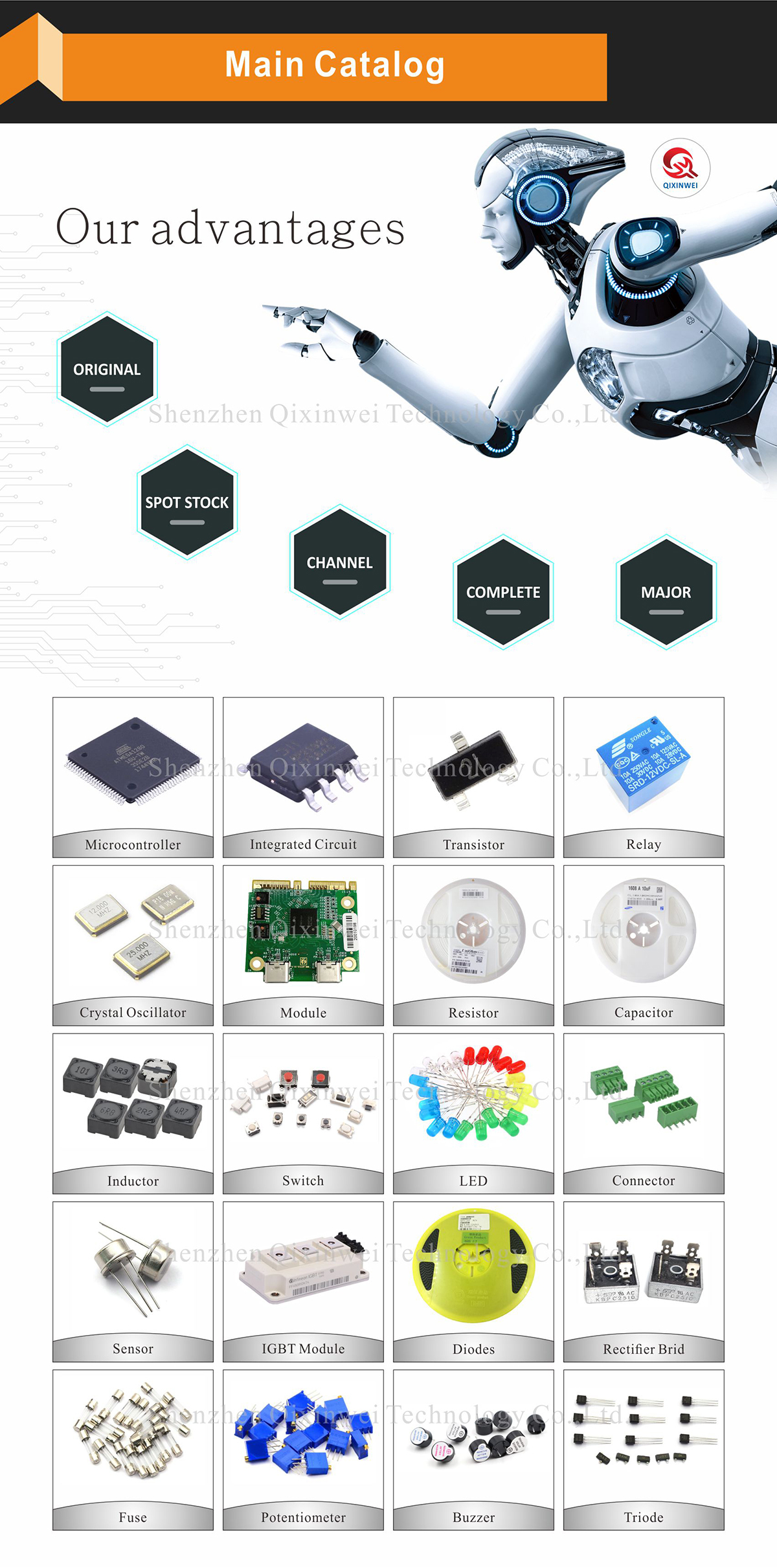
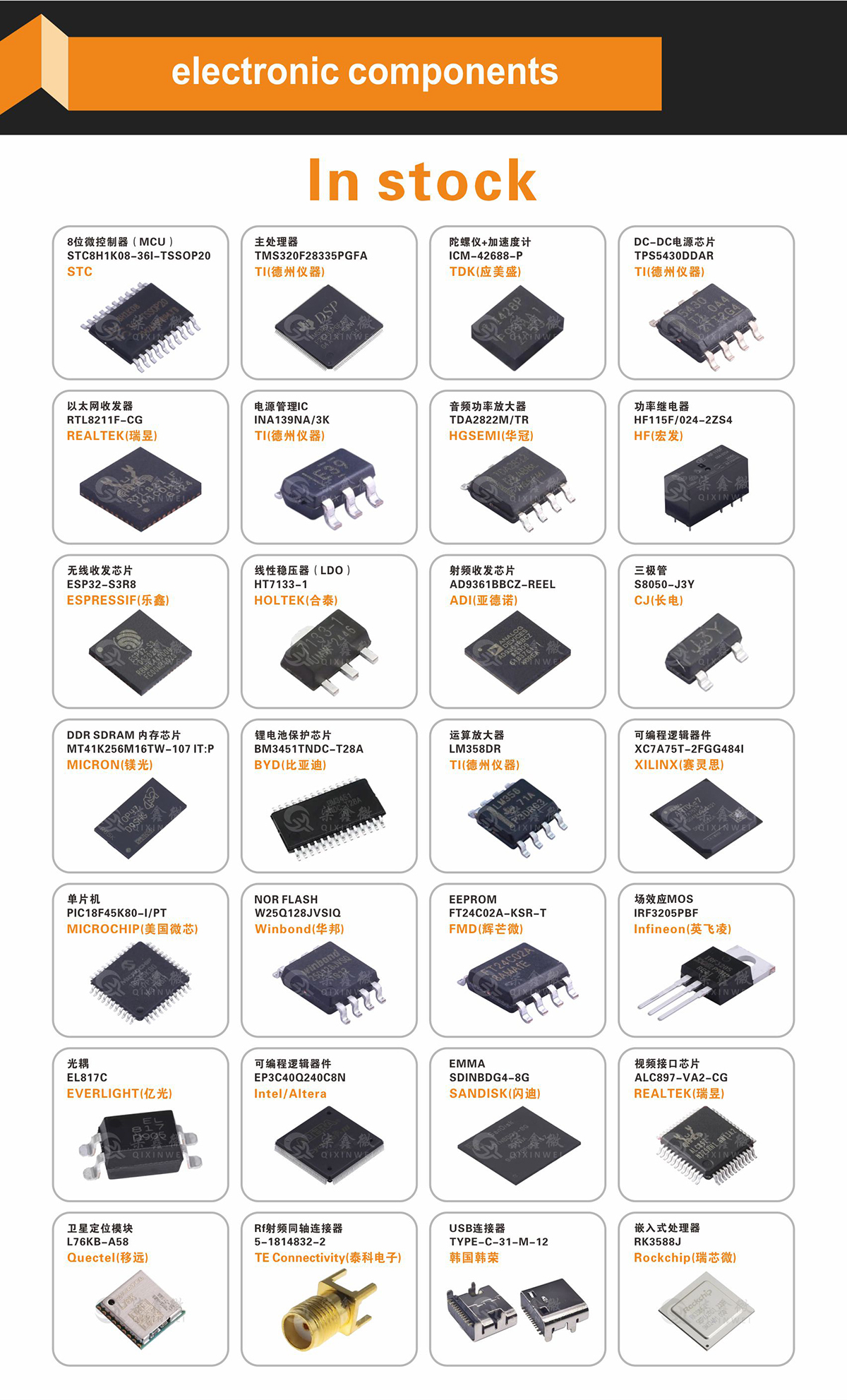
Massive In-Stock Inventory – Ready to ship promptly
BOM Matching Service – One-stop solution, save time
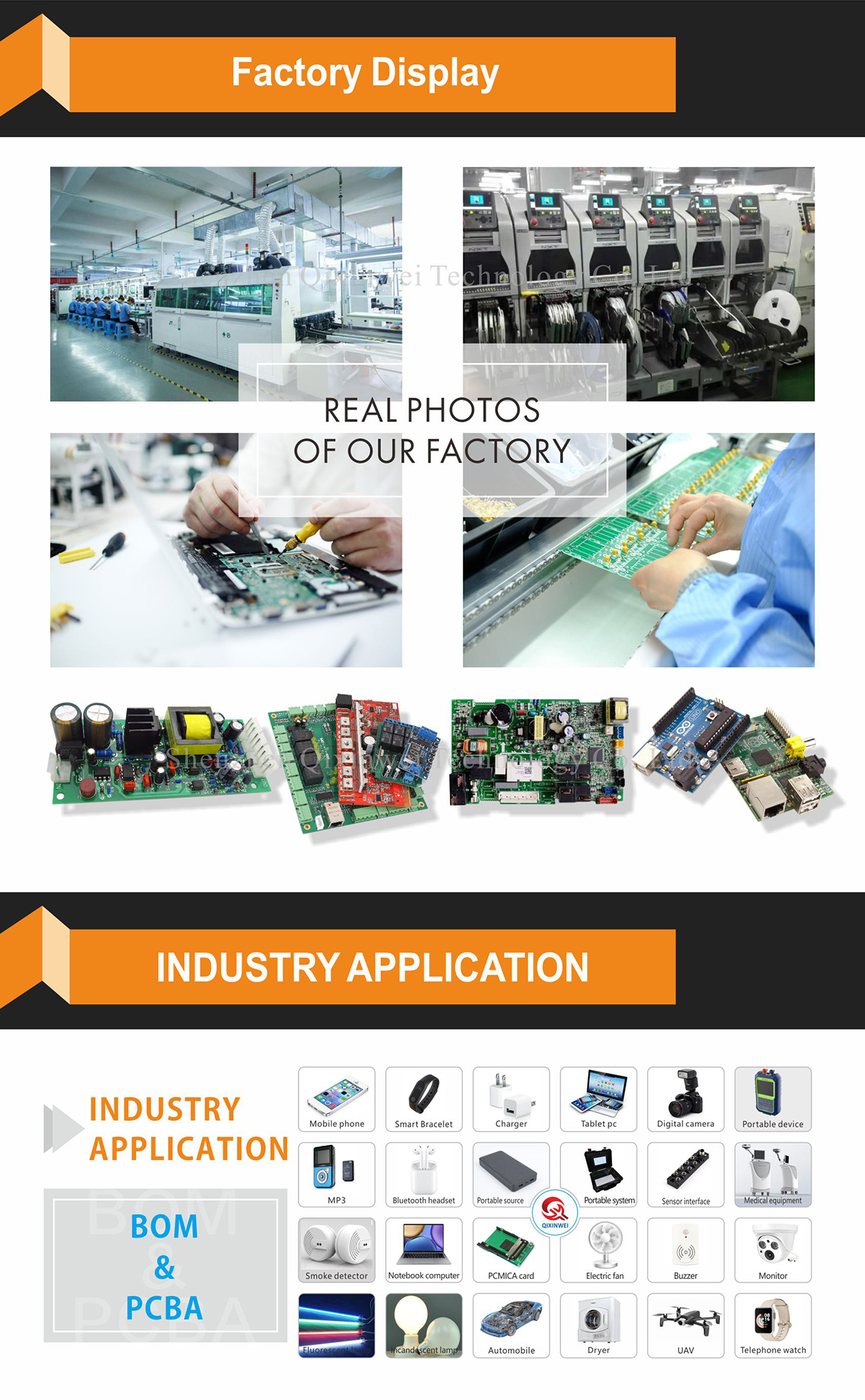
PCBA Customization – Professional engineering team creates tailor-made solutions based on your needs
Cost-Effective & Efficient – Better channel, better cost
A dedicated team makes your procurement smoother.
Contact us for BOM quotes or PCBA inquiries





FAQ:
What is the STM32C031F6P6 and what are its key specifications?
The STM32C031F6P6 is a 32‑bit microcontroller from STMicroelectronics, built around an ARM Cortex‑M0+ core running at up to 48 MHz. It offers 32 KB of Flash memory and a generous 12 KB of SRAM. On‑chip peripherals include a 12‑bit 1 Msps ADC, a TIM1 timer with one complementary PWM pair, plus general‑purpose timers (TIM3, TIM14, TIM16, TIM17), and standard serial interfaces — USART, SPI, and I2C. It is housed in a compact TSSOP‑20 package with 15 I/O pins and operates over ‑40 °C to +85 °C. As part of the STM32C0 series, this MCU delivers an excellent balance of large SRAM, small Flash footprint, and easy hand‑soldering for cost‑sensitive, space‑constrained applications.What are the package dimensions and I/O count of the STM32C031F6P6?
The device uses a TSSOP‑20 package with a body size of 6.5 mm × 4.4 mm and a lead pitch of 0.65 mm. It provides 15 general‑purpose I/O pins, which is typical for a 20‑pin package. The gull‑wing leads are easy to hand‑solder, inspect, and even use with breadboard adapters, making this chip very popular for rapid prototyping, educational projects, and low‑volume production.How does the STM32C031F6P6 differ from the STM32C031F4P6? Which one should I choose?
Both share exactly the same core, 12 KB SRAM, peripherals, and TSSOP‑20 package with 15 I/O pins. The only difference is the Flash size: the F6P6 offers 32 KB of Flash, while the F4P6 provides 16 KB. If your firmware fits comfortably within 16 KB, the F4P6 is a highly cost‑optimized option. If you need the extra code space for communication stacks, more complex logic, or future updates, the F6P6 gives you twice the Flash without any PCB change.How does the STM32C031F6P6 compare with the STM32F031F6P6? What are the main improvements?
Both are 32 KB Flash MCUs in a TSSOP‑20 package with 15 I/O pins. The C031F6P6 upgrades the core to the more efficient ARM Cortex‑M0+ and triples the SRAM from 4 KB (on the F031) to 12 KB. This extra RAM is a huge benefit for data buffering, communication stacks, or a lightweight RTOS. The timer configuration is different: the F031F6P6 has a full TIM1 with four complementary PWM pairs, while the C031F6P6 has TIM1 with just one complementary pair. Choose the C031F6P6 when you need more SRAM and better power efficiency; choose the F031F6P6 if you need three‑phase motor control in the same small package.Does the STM32C031F6P6 have a motor‑control timer? Can it drive a brushless motor directly?
It includes a TIM1 timer with one complementary PWM pair, programmable dead‑time insertion, and a break input. This single complementary channel can directly drive a single half‑bridge or an H‑bridge, making it well‑suited for DC motor control, single‑phase inverters, or PFC stages. A three‑phase brushless motor requires three complementary pairs, so the C031F6P6 cannot drive one by itself. You would need external gate drivers that handle dead‑time and complementary generation, or you can move to an MCU with a full four‑pair TIM1, such as the STM32F031F6P6 or the STM32G431 series.What are the ADC specifications of the STM32C031F6P6? How many analog input channels can I use?
It integrates a 12‑bit successive‑approximation ADC with a maximum sampling rate of 1 Msps. In the TSSOP‑20 package, up to 9 external analog input channels are available: 8 channels (IN0–IN7) through PA0–PA7, and 1 channel (IN9) via PB1. The ADC can also sample the internal temperature sensor and the internal voltage reference without consuming any external pins. There is no on‑chip DAC, so analog outputs must be implemented with an external DAC or by low‑pass filtering a PWM signal.Can the STM32C031F6P6 be powered directly from 5 V? Are its GPIOs 5‑volt tolerant?
The supply voltage must remain within 2.0 V to 3.6 V; 5 V must never be applied to the VDD pin. Most I/O pins (ports A, B, and C) are marked as FT (5‑volt tolerant) and can safely accept input voltages up to 5 V. This allows you to directly connect 5 V logic devices — reading their outputs or using open‑drain outputs with external pull‑ups — without external level shifters, significantly simplifying mixed‑voltage designs.How low is the power consumption of the STM32C031F6P6? Is it suitable for battery operation?
The Cortex‑M0+ core provides very good energy efficiency. In Run mode at 48 MHz with all peripherals active, the typical current is around 10–12 mA. Sleep mode reduces this to roughly 2–3 mA. In Stop mode, with the full 12 KB SRAM and registers retained, the current drops to about 3–5 µA; Standby mode lowers it further to approximately 0.6 µA. Fast wake‑up from Stop mode makes the MCU ideal for battery‑powered devices that sleep most of the time and wake only briefly to measure, process, and transmit data.How do I program and debug the STM32C031F6P6? What development tools are needed?
Programming and debugging are performed through the SWD (Serial Wire Debug) interface, requiring only SWDIO, SWCLK, VCC, and GND connections. A low‑cost ST‑LINK/V2 or STLINK‑V3 debugger is the only essential hardware. The free STM32CubeIDE offers full support, and the chip also works with Keil MDK and IAR EWARM. Use STM32CubeMX for fast graphical pinout, clock, and peripheral configuration. ST provides comprehensive HAL and LL libraries along with many example projects, enabling a very rapid transition from concept to prototype.What are the most typical applications for the STM32C031F6P6?
With its large 12 KB SRAM, 32 KB Flash, 15 I/O pins, and easy‑to‑solder TSSOP‑20 package, the C031F6P6 is an excellent fit for compact, cost‑sensitive designs that need generous RAM but only a modest number of I/Os. Typical uses include smart sensors, simple IoT edge nodes, battery chargers, small home appliances, power tools, and basic industrial controllers. It is especially attractive for battery‑powered projects that require communication buffers or a lightweight RTOS, where the 12 KB SRAM is a major advantage over legacy 4 KB parts.
- Product Type:
- Mainstream Arm Cortex-M0+ 32-bit MCU
- Brand:
- STMicroelectronics
- Series:
- STM32C0
- Core:
- Arm Cortex-M0+ 48MHz
- Package:
- TSSOP-20 (4.40 mm width)
- Memory:
- 32KB Flash, 12KB SRAM
- Peripherals:
- 12-bit ADC (2.5MSps/21ch), Advanced motor control timer, 4 GP timers, Low-power RTC, CRC
- Interfaces:
- I2C (1 Mbit/s), SPI (24 Mbit/s, I²S mux), 2x USART (with LIN/IrDA)
- Voltage:
- 2.0V~3.6V
- Temperature:
- -40°C~85°C


