
qixinwei-pcba


RK860-2 Rockchip DC-DC Buck Converter IC 7A High Current 2.4MHz WLCSP-20
RK860-2 Product Overview
The RK860-2 is a next-generation high-efficiency synchronous step-down DC-DC converter from Rockchip, housed in an ultra-compact WLCSP-20 package (1.61×2.01mm). It is the highest output current model in the RK860 series, designed for high-performance processor core power applications. Delivering up to 7A output current, it meets the demanding power requirements of NPU and CPU clusters in flagship processors like the RK3588.
The RK860-2 operates from a 2.7V to 5.5V input voltage range. The output voltage is I²C programmable from 0.5V to 1.5V (6.25mV/step) or 0.7125V to 1.5V (12.5mV/step). Featuring synchronous rectification with built-in low RDS(ON) power switches (24mΩ PFET) and 2.4MHz switching frequency, it achieves over 90% efficiency at 7A load. The device operates from -40°C to +125°C junction temperature with only 70μA quiescent current.
RK860-2 Core Features
7A Ultra-High Output Current: Delivers up to 7A maximum output, the highest current rating in the RK860 series, meeting demanding core power requirements of flagship processors
Wide Range Programmable Output Voltage: I²C programmable output from 0.5V to 1.5V (6.25mV/step) or 0.7125V to 1.5V (12.5mV/step) for industry-leading voltage regulation accuracy
Wide Input Voltage Range: 2.7V to 5.5V compatible with Li-ion batteries, USB power, and 5V adapters
2.4MHz High Switching Frequency: Allows ultra-compact inductors (0.24µH) and ceramic capacitors, significantly reducing power module footprint
High Efficiency Synchronous Rectification: Built-in 24mΩ PFET switch eliminates external Schottky diode, achieving over 90% efficiency at 7A
Ultra-Compact WLCSP Package: WLCSP-20 measuring just 1.61×2.01mm with 0.39mm height, ideal for ultra-thin portable devices
Ultra-Low Quiescent Current: Only 70μA typical quiescent current extends battery life in portable applications
Optimized External Components: Designed for 0.24µH inductor and 22µF×2 ceramic capacitors for minimal peripheral count
I²C Programmable Interface: Real-time output voltage adjustment supporting Dynamic Voltage Scaling (DVS) for power optimization
Industrial Wide Temperature Range: -40°C to +125°C junction temperature for industrial and outdoor applications
RK860-2 Applications
Flagship Processor Core Power: Core power supply for NPU and CPU clusters in RK3588 and other high-end processors with 7A capability
High-Performance Compute Modules: Core power for SoMs, AI accelerators, and FPGAs requiring high-density computing power
Ultra-Thin Tablets/2-in-1 Devices: Ultra-compact package with 0.24µH inductor enabling power module footprint under 10×10mm
IoT Gateways/Edge Computing: Wide temperature operation with low quiescent current for 24/7 outdoor gateway applications
Smart Wearables/Portable Devices: 70μA quiescent current extends battery life with compact package for tight spaces
Embedded Single Board Computers: Industrial-grade power for SBCs and industrial control CPU core power
RK860-2 Key Advantages
Highest Current in RK860 Series: 7A output capability is the highest in the RK860 series, optimized for flagship processors like RK3588 NPU and CPU clusters
Industry-Leading Programmable Voltage Precision: I²C interface enables 6.25mV/step or 12.5mV/step output adjustment for fine-grained core voltage control with DVS support
Exceptional Power Density: 7A output from 1.61×2.01mm WLCSP-20 package delivers unmatched power density for high-density PCB designs
2.4MHz High Frequency for Minimal External Components: 0.24µH inductor with 0603/0402 footprint and only 22µF×2 output capacitors — fewer than 8 total external components
24mΩ Low RDS(ON) for High Efficiency: Built-in 24mΩ PFET minimizes conduction loss at high currents, controllable heat generation even at 7A
70μA Ultra-Low Quiescent Current: 70μA Iq with DVS reduces PMIC power consumption by 30-40% during system standby
Deeply Optimized for Rockchip Flagship Processors: Voltage range and timing perfectly matched with RK3588 core power requirements. Production-validated in multiple mass-produced products
Mature WLCSP Assembly Process: 0.4mm ball pitch supports standard SMT reflow with high yield. Ultra-compact 1.61×2.01mm footprint fits on fingertip-sized PCB areas
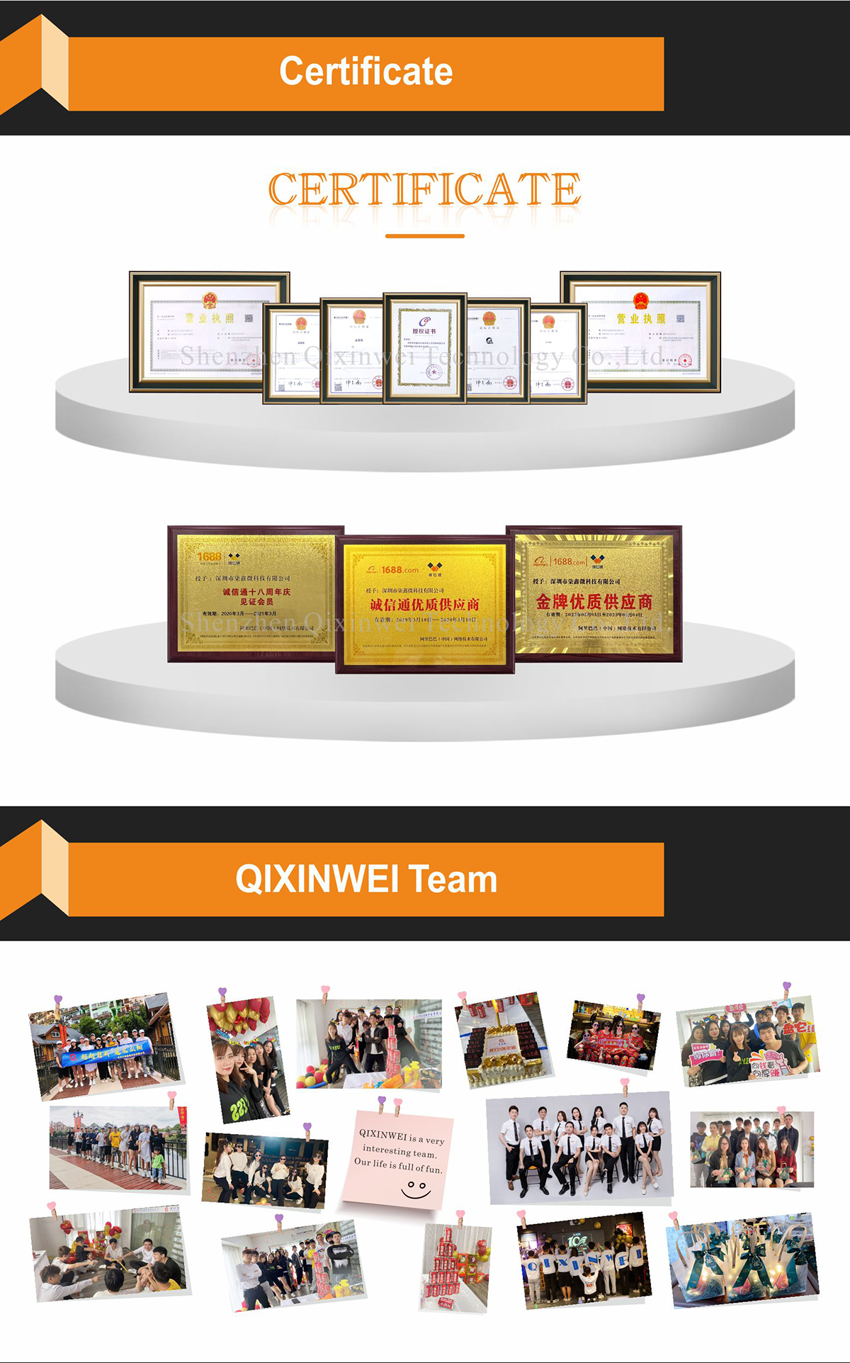
Why Choose QIXINWEI
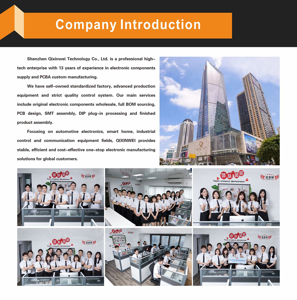
Years of experience in the electronics industry. Trusted by global customers.
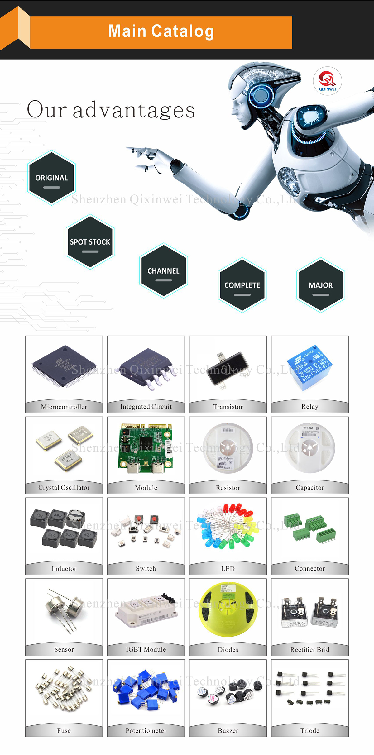
Massive In-Stock Inventory – Ready to ship promptly
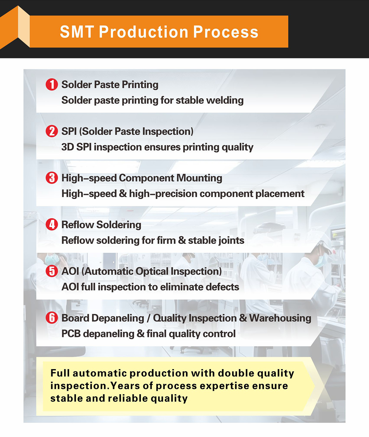
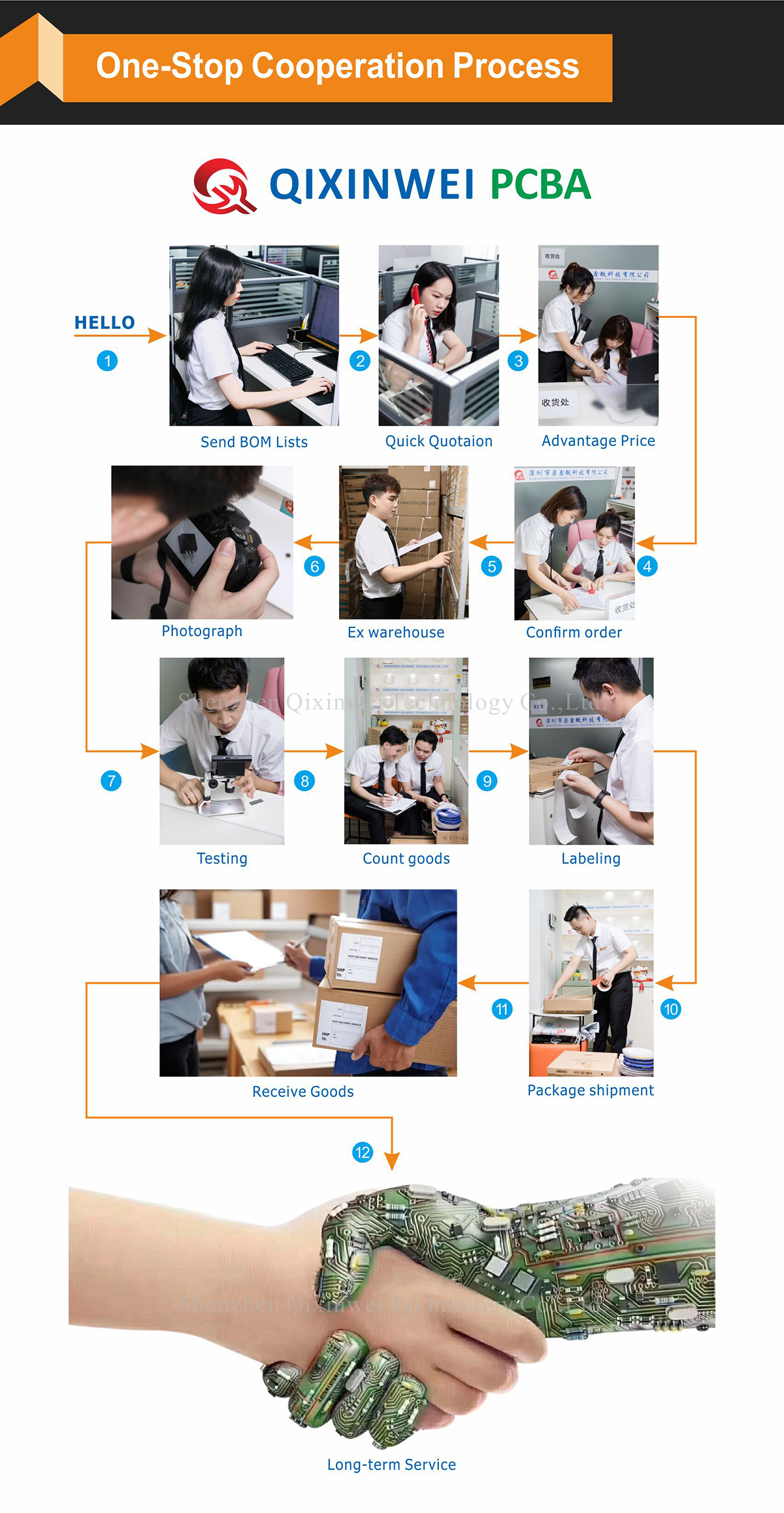
BOM Matching Service – One-stop solution, save time
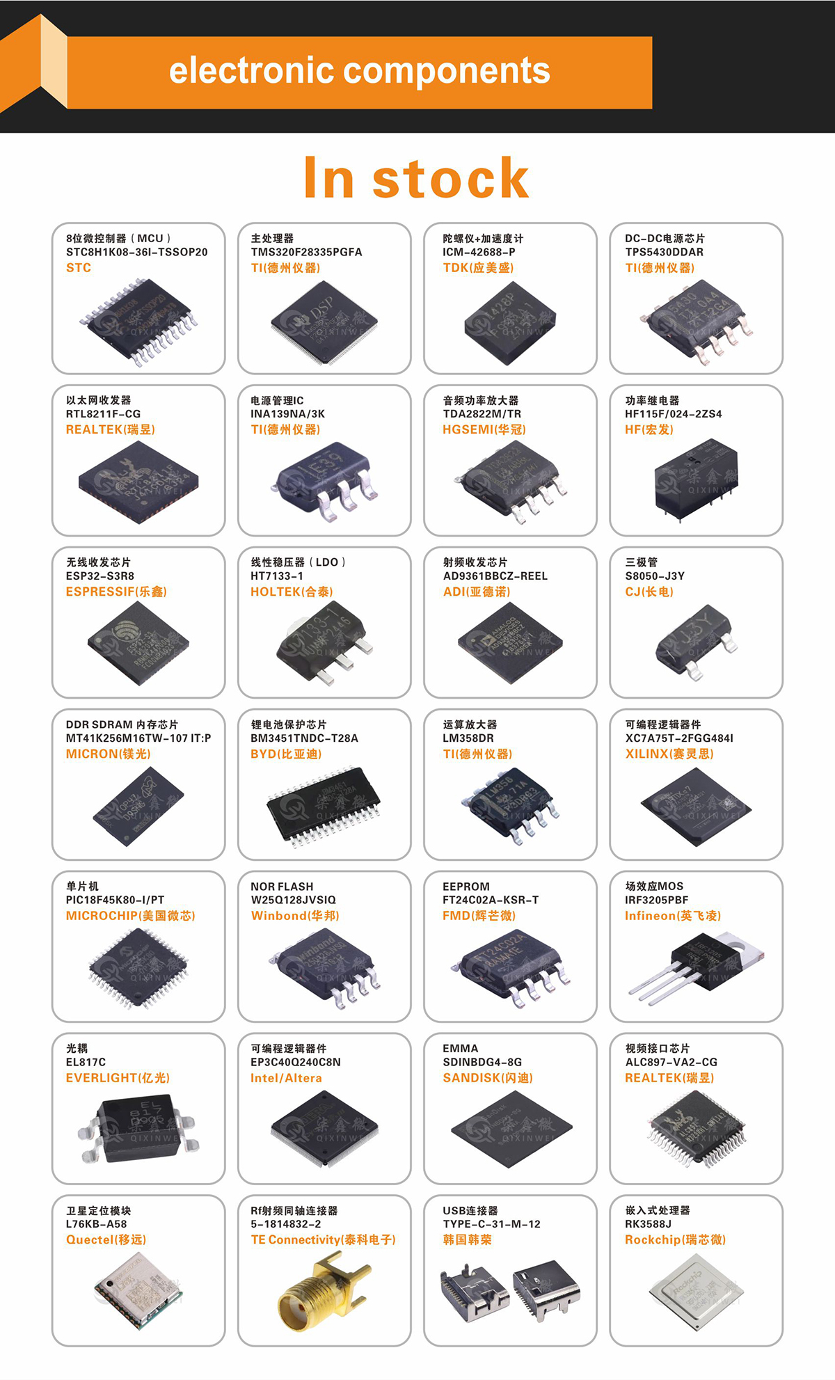
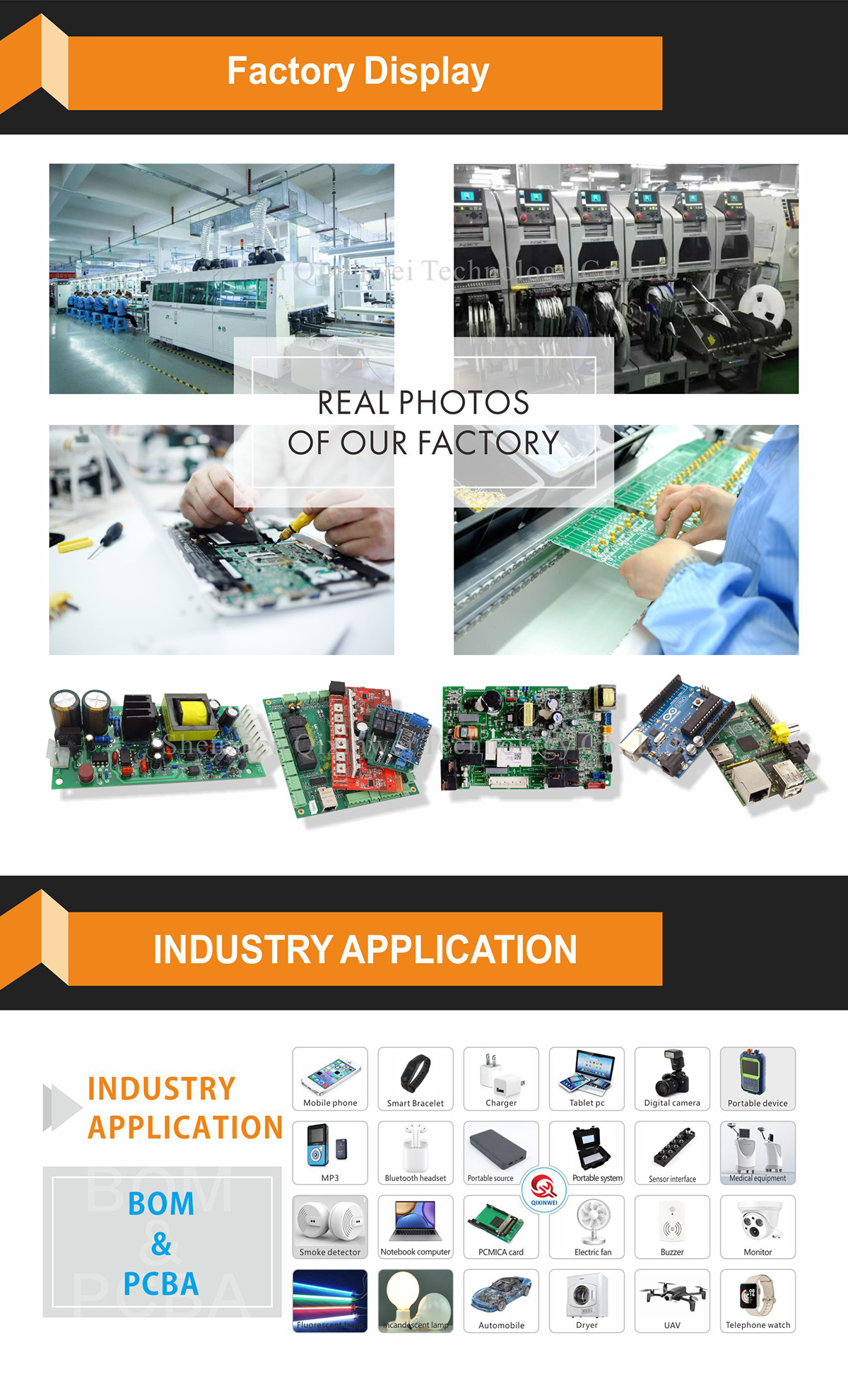
PCBA Customization – Professional engineering team creates tailor-made solutions based on your needs
Cost-Effective & Efficient – Better channel, better cost
A dedicated team makes your procurement smoother.
Contact us for BOM quotes or PCBA inquiries!



FAQ:
What is the RK860-2 and its key specifications?
The RK860-2 is a high‑performance DC‑DC synchronous buck converter from Rockchip, designed to deliver up to 7 A of continuous output current. It operates at a fixed 2.4 MHz switching frequency, enabling the use of tiny inductors and capacitors. Key features include an input voltage range of 2.7 V – 5.5 V, an adjustable output voltage (typically 0.6 V – 1.4 V via I2C), integrated power MOSFETs, and a very small WLCSP‑20 package (approximately 1.63 mm × 2.03 mm). It achieves up to 95 % peak efficiency and is optimized for powering high‑performance SoCs, FPGAs, and other digital loads in space‑constrained designs.How much output current can the RK860-2 supply?
The RK860-2 is rated for a continuous output current of 7 A. It can handle higher peak currents for short durations, making it suitable for processors with bursty power demands. The integrated power MOSFETs and advanced thermal design allow it to deliver full current without an external heatsink, provided adequate PCB copper area is available for heat dissipation.What is the switching frequency and why is 2.4 MHz beneficial?
It operates at a fixed 2.4 MHz switching frequency. This high frequency significantly reduces the size of the required inductor and output capacitor — typically a 0.47 µH inductor and small ceramic capacitors. A high frequency also moves switching noise well above the audio band and allows faster transient response, making the design very compact while still delivering 7 A of current.How can I adjust the output voltage of the RK860-2?
The output voltage is programmed via an I2C interface. You can dynamically set the output voltage to a specific value within the supported range (typically from 0.6 V to 1.4 V in small steps). This digital control removes the need for external feedback resistors and allows the system to adjust the core voltage for power‑saving modes (e.g., DVFS) under software control.What is the efficiency of the RK860-2 and how does it achieve such high efficiency?
It can reach a peak efficiency of up to 95 %. The high efficiency is achieved through integrated low‑RDS(on) MOSFETs, synchronous rectification, and optimized gate drivers. At light loads, it automatically enters a power‑saving mode (PFM) to maintain high efficiency. The 2.4 MHz operation and small WLCSP package minimize parasitic losses, keeping thermal dissipation low even at full 7 A load.What protection features does the RK860-2 include?
The RK860-2 includes a comprehensive set of protection features: over‑current protection (OCP) on a cycle‑by‑cycle basis, over‑temperature protection (OTP) with hysteresis, under‑voltage lockout (UVLO) on the input, and output over‑voltage protection (OVP). It also supports soft‑start to limit inrush current and a power‑good (PG) flag to indicate when the output is in regulation. These features ensure safe operation in demanding applications.What is the input voltage range and what supplies can power the RK860-2?
The input voltage range is 2.7 V to 5.5 V. This makes it compatible with common single‑cell Li‑ion batteries (3.0 V – 4.2 V), 5 V USB rails, and standard 3.3 V or 5 V system supplies. The wide input range gives flexibility to use the same converter in battery‑powered devices as well as mains‑powered equipment.How small is the WLCSP‑20 package, and what does it mean for PCB design?
The WLCSP‑20 package measures only 1.63 mm × 2.03 mm, with a 0.4 mm ball pitch. This ultra‑compact size, combined with the high switching frequency, creates a total solution footprint of less than 50 mm². It is ideal for smartphones, tablets, wearables, and any design where board space is at a premium. Because it is a wafer‑level package, it also exhibits very low parasitic inductance, contributing to the high efficiency and low EMI.How does the RK860-2 compare to a traditional high‑current LDO regulator?
An LDO capable of 7 A would dissipate enormous heat — for a 5 V‑to‑1 V conversion, it would waste 28 W of power and require a massive heatsink. The RK860-2 operates as a switching regulator with ~95 % efficiency, wasting only about 0.35 W at 7 A/1 V output. This makes it dramatically cooler, smaller, and more battery‑friendly. For any high‑current application, a buck converter like the RK860-2 is the only practical choice.What are the most typical applications of the RK860-2?
It is commonly used to supply core and I/O voltages for high‑performance Rockchip SoCs (e.g., RK3588, RK3568), FPGAs, AI accelerators, and other power‑hungry digital chips. Because of its tiny size, it is a popular choice in smartphones, tablets, AIoT edge devices, drones, and portable instruments. The combination of 7 A capacity, I2C programmability, and a WLCSP package makes it an excellent power management IC for modern compact electronics.
- Manufacturer:
- Rockchip
- Model Number:
- RK860-2
- Product Type:
- DC-DC Step-Down Power Converter IC
- Function Type:
- Step-Down (Buck)
- Synchronous Rectification:
- Yes
- Input Voltage:
- 2.7V to 5.5V
- Output Voltage:
- 0.5V to 1.5V (I²C Programmable, 6.25mV/step or 12.5mV/step)
- Output Current:
- 7A Maximum
- Number of Outputs:
- 1
- Switching Frequency:
- 2.4MHz
- Quiescent Current:
- 70μA typical
- Power Switch:
- Built-in (PFET 24mΩ)
- Operating Temperature:
- -40°C to 125°C (Junction Temperature)
- Package Type:
- WLCSP-20 (1.61×2.01mm)
- Package Dimensions:
- 2.01mm L × 1.61mm W × 0.39mm H
- Topology:
- Buck
- Output Type:
- Programmable
- Typical Companion Components:
- 0.24µH Inductor + 22µF×2 Ceramic Capacitors
- Application Grade:
- Industrial


