qixinwei-pcba


EP4CE10F17C8N Altera Cyclone IV E FPGA 10K Logic Elements 256-FBGA
EP4CE10F17C8N Product Overview
The EP4CE10F17C8N is a high cost-performance FPGA from Altera (now Intel) in the Cyclone IV E series, manufactured on 60nm low-power process technology, designed for cost-sensitive high-volume applications. The device features 10,320 Logic Elements (LEs), 645 Logic Array Blocks (LABs), 414Kbits of embedded memory, and 179 user I/O pins, operating at up to 402MHz. This commercial grade (C grade) device supports 0°C to 85°C operating temperature range and comes in a 256-pin FBGA package (17×17mm), making it ideal for industrial control, communication systems, and embedded applications.
EP4CE10F17C8N Core Features
Logic Resources: 10,320 Logic Elements (LEs) and 645 Logic Array Blocks (LABs) providing ample digital logic design capability for medium-scale circuit implementation
Embedded Memory: 423,936 total RAM bits (approx 414Kbit) for FIFO buffers, data caching, and storage applications
DSP Processing: 23 embedded 18x18 multipliers supporting DSP processing intensive applications for signal processing and filter design
I/O Interfaces: 179 user I/O pins supporting LVTTL, LVCMOS, and other standards for flexible external connectivity
Global Clock Network: 10 global clock networks ensuring low skew and high coverage
Phase-Locked Loops: 2 general purpose PLLs supporting clock synthesis, multiplication, division, phase shifting, and programmable duty cycle
LVDS Interfaces: Supports LVDS receiver up to 875 Mbps and transmitter up to 840 Mbps
External Memory Interfaces: Supports DDR2 SDRAM up to 200MHz, QDRII SRAM and DDR SDRAM up to 167MHz
Maximum Frequency: Internal logic up to 402MHz, I/O data rates up to 1.6Gbps
Supply Voltage: Core voltage 1.15V to 1.25V (1.2V typical), I/O voltage 1.5V to 3.3V multi-voltage support for low power design
Package Type: 256-pin FBGA (17×17mm) with 1.0mm ball pitch, surface mount, lead free RoHS compliant
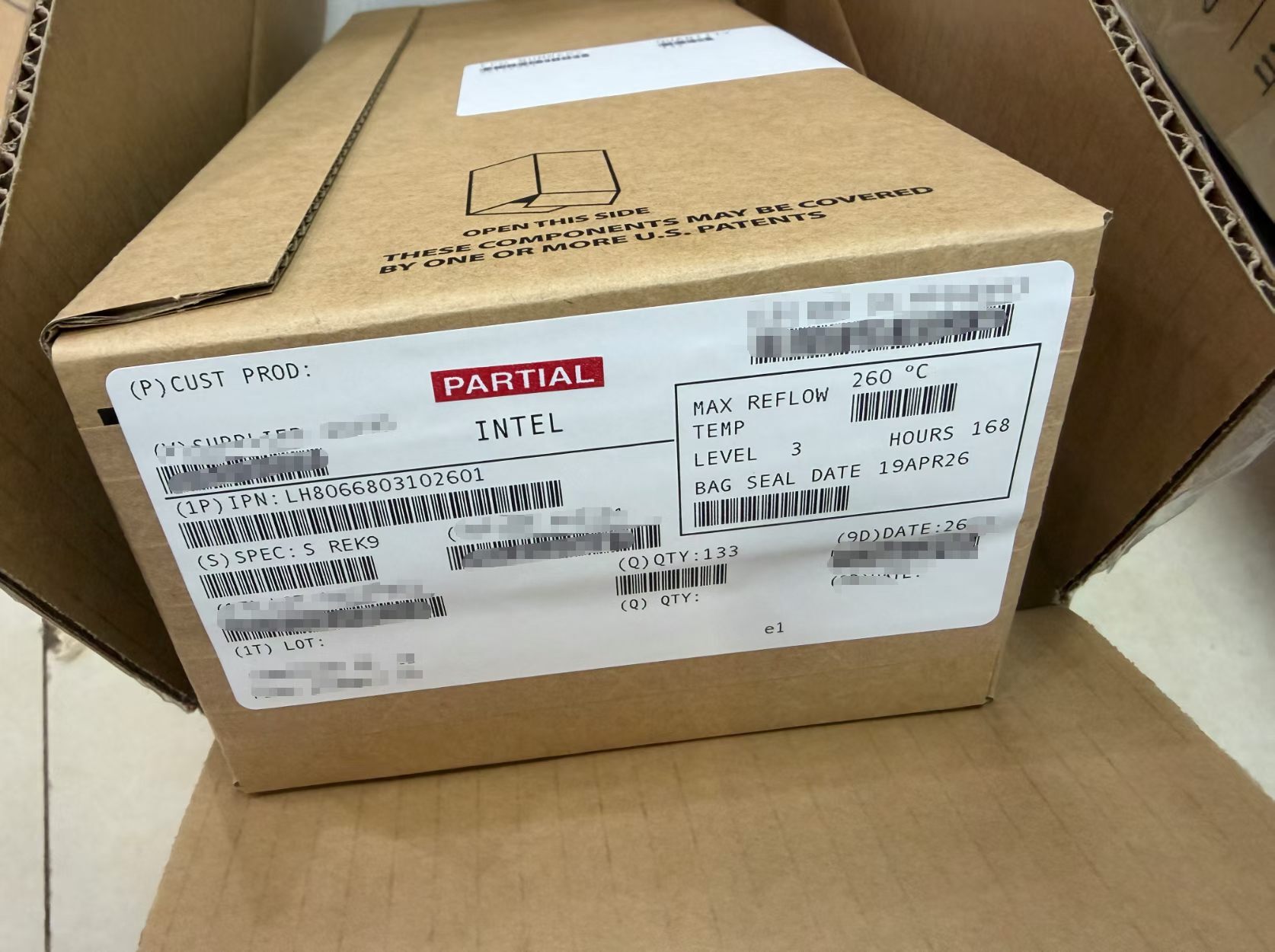
Temperature Range: Commercial grade 0°C to 85°C with MSL Level 3 (168 hours)
Bitstream Security: Support for configuration bitstream encryption to protect design IP
Program Cycles: Supports over 100,000 program erase cycles
EP4CE10F17C8N Applications
Industrial Control: PLC systems, motion controllers, automation equipment, machine vision, industrial robotics
Communication Systems: Protocol converters, data buffering, interface bridging, UART/SPI expansion, Gigabit Ethernet interfaces
Consumer Electronics: Smart home control, audio/video processing modules, display control systems, gaming peripherals
Embedded Systems: Logic expansion, interface conversion, data acquisition preprocessing working with MCU/ARM processors
Data Acquisition: Industrial field data acquisition, sensor signal processing, edge computing preprocessing
Automotive Electronics: In-vehicle infotainment interfaces, ADAS auxiliary processing
Medical Devices: Medical imaging front-end processing, portable medical device logic control
EP4CE10F17C8N Key Advantages
High Cost-Performance FPGA: Cyclone IV series is Altera's classic low-cost family, EP4CE10F17C8N offers competitive pricing at 10K logic scale (volume pricing approximately 41.83), making it ideal for cost-sensitive high-volume applications, with refurbished channel pricing reaching 15, significantly lowering the entry barrier
Low Power Design: 60nm low-power process with total power under 1.5W for protocol bridging applications, lower core current suitable for energy-sensitive systems and portable devices
Flexible Programmability: FPGA core advantage is reconfigurability, supporting Verilog/VHDL design, logic functions can be modified without hardware changes, greatly reducing development cycles and prototyping time
Balanced Resource Allocation: The balanced combination of 10K logic elements, 23 DSP multipliers, 414Kbit RAM, and 179 I/Os is ideal for medium complexity logic designs, neither excessive nor insufficient
Rich I/O Resources: 179 user I/O pins support multiple standards including LVTTL, LVCMOS, SSTL, HSTL, easily connecting to ADCs, DACs, displays, and communication modules
High-Speed Interface Capability: Supports LVDS up to 875Mbps, DDR2 interface up to 200MHz, overall I/O data rates up to 1.6Gbps for high-speed data transmission
Mature Design Tool Support: Intel Quartus II/Prime design suite provides complete development environment and rich IP core support
Stable Supply Chain: With abundant global inventory, the device supports long-life project procurement needs
Lead Free Environmentally Friendly Package: RoHS compliant with lead free process meeting environmental regulations
Beginner-Friendly Learning Platform: The moderate scale of logic resources, ample I/O, and mature tool chain make it an ideal entry-level platform for FPGA beginners
Why Choose QIXINWEI
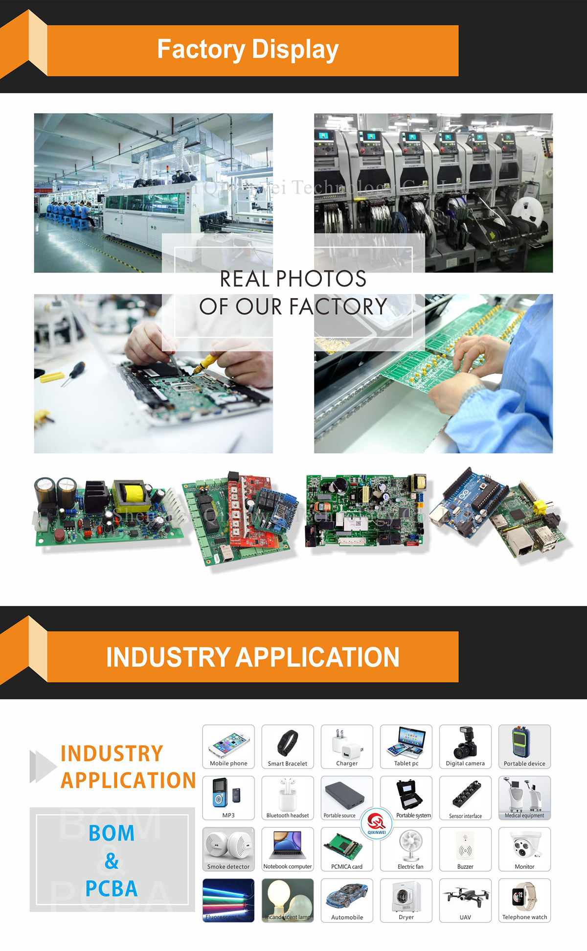
Years of experience in the electronics industry. Trusted by global customers.
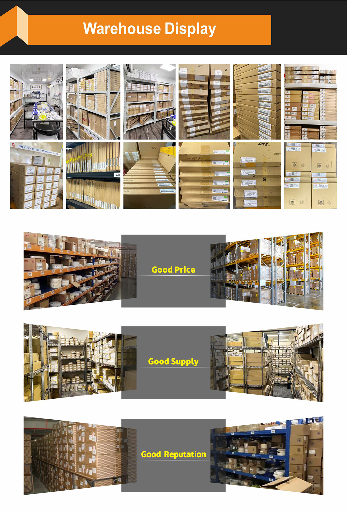
Massive In-Stock Inventory – Ready to ship promptly
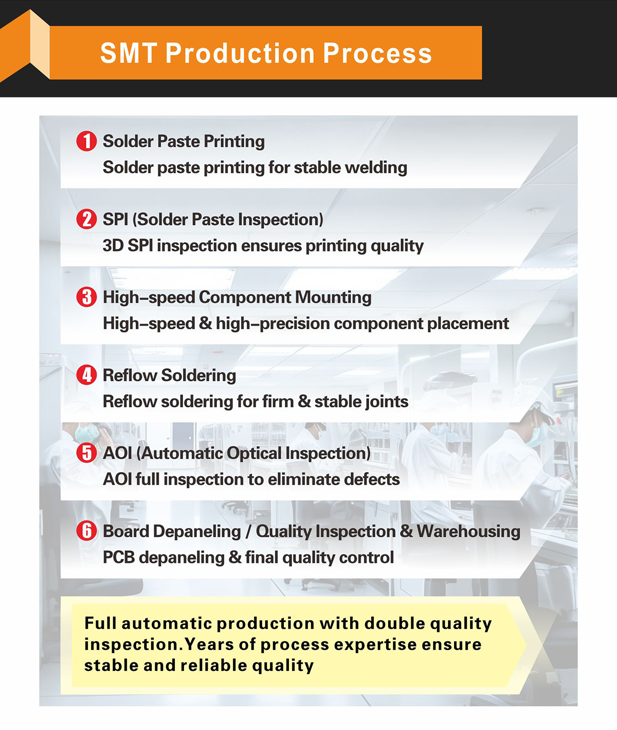
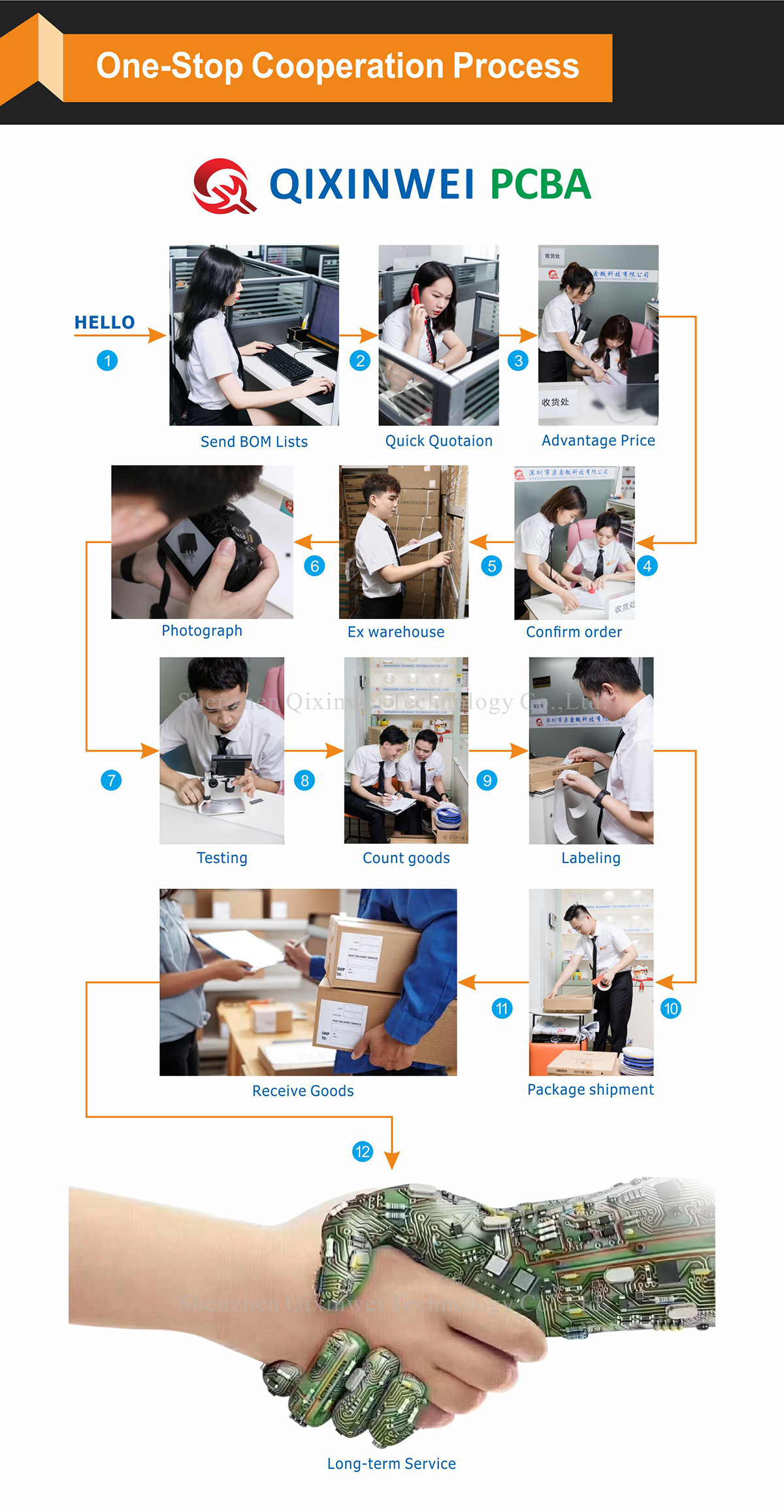
BOM Matching Service – One-stop solution, save time
PCBA Customization – Professional engineering team creates tailor-made solutions based on your needs
Cost-Effective & Efficient – Better channel, better cost
A dedicated team makes your procurement smoother.
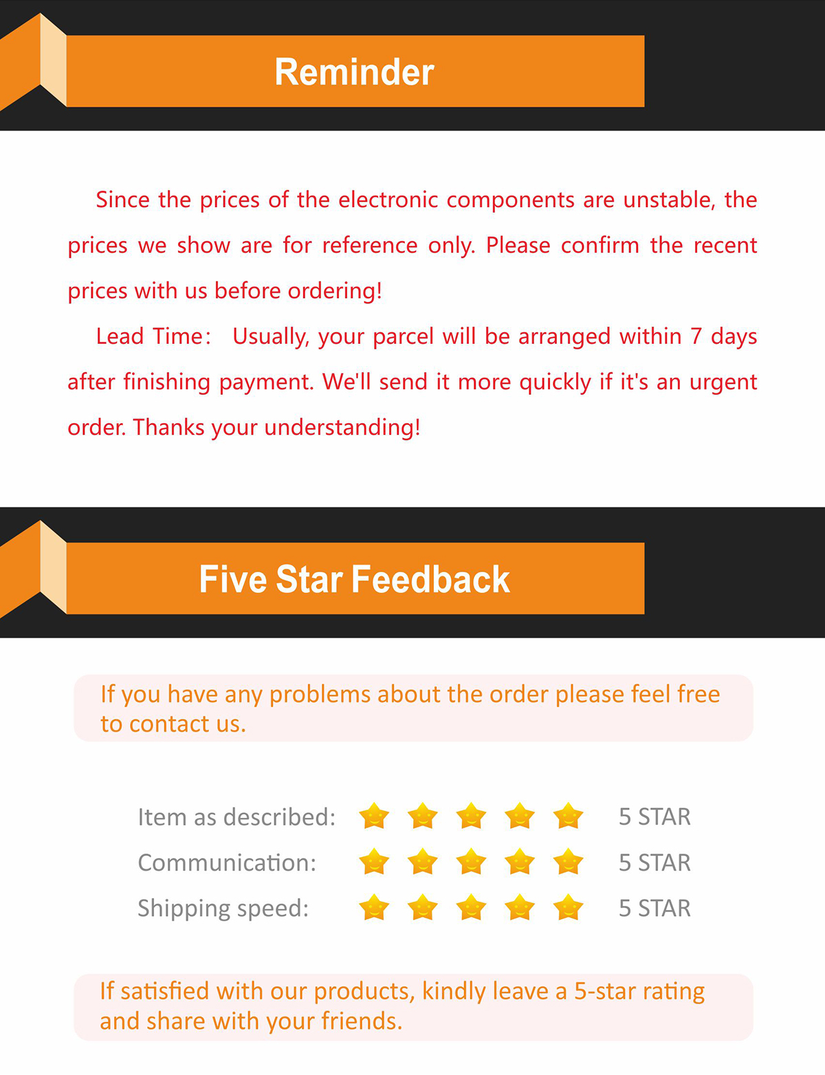
Contact us for BOM quotes or PCBA inquiries




FAQ:
What is the EP4CE10F17C8N and its key specifications?
This is an Altera Cyclone IV E FPGA built on a low‑power 60 nm process. It provides 10,320 logic elements (LEs), 414 Kbits of embedded block RAM, 23 18×18 hardware multipliers, and 2 general‑purpose PLLs. The device is housed in a 256‑pin FineLine BGA (FBGA256) package, offering up to 179 user I/O pins. It supports a wide range of single‑ended and differential I/O standards, operates from a single 1.2 V core voltage, and the “C8” speed grade indicates the fastest commercial‑grade speed bin. The “N” suffix designates a lead‑free package. This FPGA is designed for cost‑sensitive, high‑volume applications in industrial, automotive, and consumer electronics that need a moderate amount of logic and flexible I/O.How does the EP4CE10 compare to the smaller EP4CE6 in the Cyclone IV E family?
Both are members of the Cyclone IV E family and share the same process, core voltage, and I/O capabilities. The primary difference is logic density: the EP4CE10 provides 10,320 logic elements, roughly 1.6× more than the EP4CE6’s 6,272 LEs. The EP4CE10 also offers more block RAM (414 Kbits vs. 270 Kbits) and slightly more multipliers. Both are pin‑compatible within the same package (e.g., both can use the 256‑pin FBGA), making it easy to scale a design up or down. Choose the EP4CE10 when you need extra logic, more memory, or more DSP resources; the EP4CE6 is a perfectly cost‑optimised choice for smaller designs.How many I/O pins does the FBGA256 package provide, and what standards are supported?
The FBGA256 package delivers up to 179 user I/O pins. These I/Os are organised in eight banks that can be independently powered, supporting a broad set of standards: LVTTL, LVCMOS (3.3 V, 2.5 V, 1.8 V, 1.5 V, 1.2 V), SSTL, HSTL, LVDS, RSDS, and PCI. The I/O pins feature programmable slew rate, drive strength, and on‑chip termination (OCT), allowing direct connection to DDR2/DDR3 memory, legacy buses, and high‑speed LVDS links without external termination resistors. The high I/O count makes it suitable for memory‑intensive and interfacing applications.What block RAM and multiplier resources does the EP4CE10 include?
The FPGA contains 414 Kbits of embedded block RAM, arranged as 46 M9K memory blocks. Each M9K can be configured as single‑port, dual‑port, or FIFO memory. Additionally, it includes 23 dedicated 18×18 multipliers capable of operating up to 250 MHz (C8 speed grade). These multipliers are ideal for implementing digital filters, FFTs, and other moderate‑complexity DSP functions. Combined with the logic fabric, the device can efficiently handle many signal‑processing and control tasks.What does the “C8” speed grade mean, and what is the maximum performance?
The C8 speed grade is the fastest commercial temperature option for Cyclone IV E devices. It guarantees a maximum propagation delay through the logic fabric that is shorter than the C6 and C7 grades, enabling higher clock frequencies. For example, typical system performance can reach 200 MHz to 250 MHz for many designs, depending on the specific logic utilization. The “C” indicates a commercial temperature range of 0 °C to +85 °C. Choose the C8 when you need the maximum possible throughput from a Cyclone IV E FPGA.How is the EP4CE10 configured and programmed? What development tools are required?
It uses SRAM‑based configuration and requires an external non‑volatile memory — typically a low‑cost SPI Flash, EPCQ serial configuration device, or a MAX II CPLD — to store the bitstream. The FPGA loads its configuration at power‑up via Active Serial (AS), Fast Passive Parallel (FPP), or JTAG interfaces. Design entry, synthesis, and place‑and‑route are performed with Intel Quartus Prime Standard Edition (the free Quartus Prime Lite Edition fully supports Cyclone IV E). A USB‑Blaster download cable is used for programming and debugging. The built‑in SignalTap II logic analyzer allows real‑time debugging of internal signals.What is the typical power consumption of the EP4CE10, and how can it be optimised?
Static power is very low, typically well under 100 mW. Dynamic power depends on design complexity and clock frequency, but for most mid‑range designs, total on‑chip power stays under 1 W. The 60 nm low‑power process and advanced power‑gating help achieve excellent performance‑per‑watt. Further power reduction can be achieved through clock gating, lowering the I/O drive strength when possible, and using the dedicated sleep mode. The device is well‑suited for power‑sensitive industrial and portable equipment.How does the Cyclone IV E compare to the Cyclone IV GX family?
The Cyclone IV E (Enhanced) series focuses on logic, memory, and I/O density, while the Cyclone IV GX (with Transceivers) adds integrated high‑speed transceivers supporting protocols like PCIe, Gigabit Ethernet, and CPRI. The EP4CE10 does not include transceivers. If your application requires high‑speed serial links (e.g., PCIe or Ethernet directly from the FPGA), the Cyclone IV GX is the better choice. For general‑purpose logic, DSP, and parallel interfaces, the Cyclone IV E provides a more cost‑effective solution with higher I/O count in smaller packages.What is the FBGA256 package size and lead pitch? Is it suitable for prototyping?
The FBGA256 package has a body size of 17 mm × 17 mm and a ball pitch of 1.0 mm. The relatively large 1.0 mm pitch makes it one of the more prototyping‑friendly BGA packages, as it allows for easier fan‑out on standard PCB technology and is compatible with many low‑cost PCB manufacturers. While not as simple to hand‑solder as a QFP, it is very manageable with a hot‑air rework station or professional assembly. This package provides a high I/O count in a reasonable footprint.What are the most typical applications for the EP4CE10F17C8N?
Thanks to its moderate logic density, abundant I/O, and low power, the EP4CE10 is widely used in industrial motor controllers, medical imaging front‑ends, video processing and display controllers, communication bridges, automotive infotainment, and low‑cost test equipment. It is a very popular FPGA for cost‑sensitive designs that have outgrown smaller CPLDs or need flexible, parallel interfacing capabilities with a proven, long‑lifecycle device.
- Product Family:
- Altera Cyclone IV E series FPGA
- Logic Elements:
- 10,320 Logic Elements (LEs), 645 Logic Array Blocks (LABs)
- Embedded Memory:
- 423,936 total RAM bits (approx 414Kbit)
- DSP Resources:
- 23 embedded 18x18 hardware multipliers
- I/O Pins:
- 179 user I/O pins
- Global Clocks:
- 10 global clock networks
- PLLs:
- 2 general purpose PLLs
- Maximum Frequency:
- 402 MHz
- Temperature Range:
- 0°C to 85°C (Commercial Grade C)
- Package Type:
- 256-FBGA (17×17mm), 1.0mm ball pitch