Electronic components
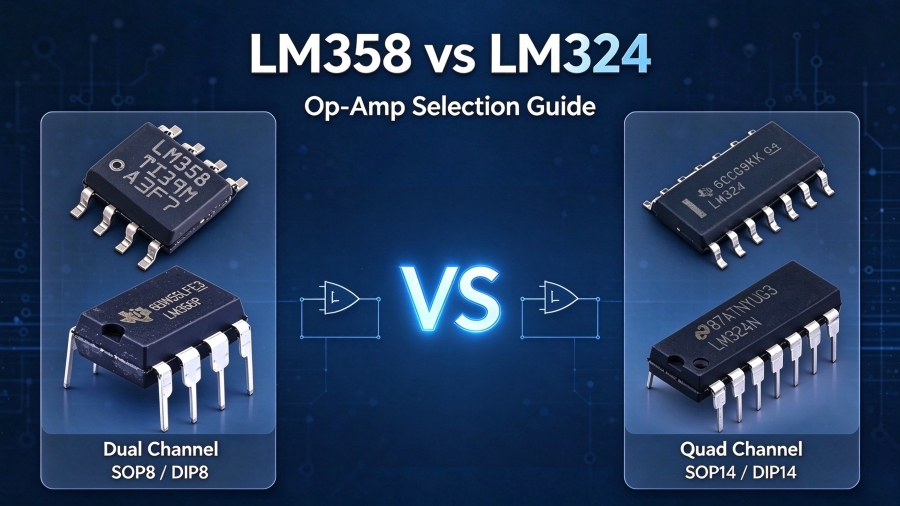
LM358 vs. LM324: A Selection Guide
I. First, Debunk a “Pseudo-Difference”: They Are the Same Chip
LM358 and LM324 have been discussed for decades, but many comparison articles spend a great deal of space on “electrical parameter differences”—which is precisely the biggest misunderstanding. According to TI’s official application notes, LM324 and LM358 share the same core silicon design, with completely identical electrical performance, supply range, and temperature grade. LM324 integrates four independent op-amp units, while LM358 has two. Their relationship can be simply remembered as: LM324 ≈ 2 × LM358.
The only difference that truly deserves serious attention is the matching of channel count and package. And there is a long-overlooked truth: the output-stage and input-stage defects shared by both are the real areas that need “pitfall avoidance” in design.
1.1 Core Comparison:
| Comparison Dimension | LM358 | LM324 |
|---|---|---|
| Number of Op-Amp Channels | 2 | 4 |
| Common Packages | DIP-8 / SOP-8 / TSSOP-8 | DIP-14 / SOP-14 |
| Power Supply Pins | Pin 4 = GND, Pin 8 = VCC | Pin 4 = VCC, Pin 11 = GND |
| Single-Supply Range | 3 V–30 V | 3 V–32 V |
| Input Offset Voltage (Typical) | 2 mV (LM358B: 3 mV max) | 3 mV (LM324B: 3 mV max) |
| Input Bias Current (Typical) | 45 nA | 20 nA |
| Output Current (Typical) | 20 mA | 40 mA |
| Gain-Bandwidth Product | 1 MHz | 1 MHz (same silicon) |
| Slew Rate | 0.4–0.6 V/µs | 0.4–0.6 V/µs |
| Output Swing (5 V Supply) | 0 V to VCC−1.5 V (about 3.5 V) | 0 V to VCC−1.7 V (about 3.3 V) |
| Crossover Distortion | Present (inherent to output stage) | Present (inherent to output stage) |
Note the key difference in power supply pins: LM358’s pin 4 is ground, while LM324’s pin 11 is ground; LM358’s pin 8 connects to VCC, while LM324’s pin 4 connects to VCC. This is not a difference that “can be fudged”—if you try to force an LM324 into an LM358 PCB position using an adapter board or flying leads, reverse power connection will directly damage the chip.
1.2 Selection Decision:
The core logic of selection is extremely direct:
Need 1–2 op-amp channels → LM358. The 8-pin package occupies the smallest PCB area, has the shortest routing, and has the lowest per-unit cost.
Need 3–4 op-amp channels → LM324. Four-channel integration minimizes the per-channel op-amp cost while reducing the number of chips and power-supply decoupling nodes on the PCB.
Need 2 channels but want room for upgrade → Evaluate LM324. If you currently need 2 channels but may expand to 3–4 in the future, using LM324 directly can avoid a board redesign, at the cost of 6 extra pins and a slightly larger package area.
But there is an easily overlooked “hidden cost”: unused op-amp channels in LM324 must not be left floating. If the inputs of unused op amps float, they may oscillate due to noise coupling and interfere with the channels in use through the power supply or substrate. The standard practice is to connect the unused op amp as a follower (non-inverting input tied to a defined mid-level, output tied to the inverting input), or at least tie the inputs to a known potential. If the “extra channels” actually bring additional design work, LM358’s “just right” may be the more economical choice.
II. The Real “Difference”: Output-Stage and Input-Stage Pitfalls Shared by Both
At the selection level, the difference between LM358 and LM324 is simple, but at the level of using them well, the challenges are shared. These two “brothers” share a bipolar output stage and a PNP Darlington input stage born decades ago, leaving several pitfalls that must be actively avoided in design.
2.1 Output Stage: Swing Limitation + Crossover Distortion—Neither Can Be Ignored
The output stage of LM358/LM324 is not rail-to-rail. With a 5 V single supply, the output high level can only reach about VCC−1.5 V (LM358) or VCC−1.7 V (LM324). The output low level can theoretically reach 0 V, but the current-sinking capability is very weak—there is only about a 50 µA internal current regulator pulling the output down to ground.
The more subtle problem is crossover distortion. The output stage uses an NPN Darlington transistor to source current and a single vertical PNP transistor to sink current. There is a dead zone at the transition point between “push” and “pull,” causing the output waveform to exhibit a nonlinear step near the zero crossing. For DC or low-speed small signals, this distortion may be hard to notice; for audio or waveforms requiring low distortion, it is a measurable error source.
The solution is straightforward: add a pull-down resistor from the output to the negative supply (GND), typically 5 kΩ–10 kΩ. This resistor forces the output stage to remain in the “sourcing” state (i.e., the PNP sinking transistor remains on), thereby bypassing the crossover dead zone and slightly improving the accuracy of the output low level. The cost is increased quiescent power consumption—in battery-powered scenarios, this cost must be included in the budget.
2.2 Input Stage: Common-Mode Range Has an Upper Limit, and Phase Reversal Must Be Watched
The input common-mode range of LM358/LM324 includes the negative supply rail (GND) but does not include the positive supply rail. Over the full temperature range, the recommended range is 0 V to VCC−2 V. This means that with a 5 V supply, the op amp will leave its linear operating region once the input signal exceeds about 3 V.
If the input is forced beyond this range, phase reversal may be triggered: the output does not saturate to the expected high level but suddenly flips to an incorrect state (usually low), causing catastrophic logic misjudgment. For sensor signal conditioning, especially where the signal swing may approach VCC, voltage division or clamping must be added before the op amp to ensure the input never exceeds the limit.
2.3 Using an Op Amp as a Comparator: Possible, but You Must “Know the Cost”
LM358/LM324 are often used as comparators because “there is an idle op amp on hand.” TI’s application note clearly states the preconditions for doing so: no strict timing requirements, inputs do not exceed the common-mode range, and the speed limitations of an op amp used as a comparator are accepted.
Op amps are designed for linear amplification and have internal compensation capacitors, with a slew rate of only 0.4–0.6 V/µs. When the input crosses the threshold, it takes microseconds for the output to swing from one rail to the other, far slower than a dedicated comparator. If the signal being compared exceeds tens of kHz, or if the system is sensitive to response delay, using LM358/LM324 as a comparator is a hidden failure point.
III. Project Cases
3.1 Case 1: Infrared Detection Alarm—2 Channels, Choose LM358
The signal chain of an infrared detection alarm usually requires two stages: the first stage amplifies the weak signal from the pyroelectric sensor, and the second stage acts as a voltage comparator to determine whether the threshold is exceeded. This is exactly the typical requirement for two op-amp channels.
The reason for choosing LM358 is space and cost: the SOP-8 package fits comfortably inside a compact alarm enclosure, and no additional inter-chip routing is needed between the two op amps. Design points include adding a pull-up resistor at the comparator output (if driving logic levels) and ensuring that the output swing of the first-stage amplifier leaves sufficient margin, avoiding the signal peak hitting the VCC−1.5 V ceiling under 5 V supply.
3.2 Case 2: Four-Channel Sensor Array Interface—4 Channels, Choose LM324
In industrial or environmental monitoring, it is often necessary to condition four sensor signals of the same type simultaneously (such as four thermocouples or four pressure bridges). If each channel uses an LM358, the board will have four chips, four sets of power decoupling, and four independent power traces, doubling PCB area and BOM complexity.
The value of LM324 here is reflected in the system simplification brought by integration: one SOP-14 package accommodates four op amps, sharing the same set of power pins and decoupling capacitors, and the layout of the four signal channels can be highly symmetrical. The cost is that you must properly handle “whether all four channels are really needed”—if only three are actually used, the unused channel must be connected as a follower with a fixed input, rather than simply left floating.
3.3 Case 3: 4–20 mA Constant Current Source—Selection Follows “Channel Count,” Design Follows “Output Stage”
In the classic implementation of a 4–20 mA industrial current loop, LM358/LM324 are often used for error amplification and driving transistors. A typical constant current source circuit may require: one error amplifier, one buffer/level shift, and possibly a monitoring channel—two channels use LM358, three or more use LM324.
But regardless of which chip is selected, the output-stage pull-down resistor and current-sinking capability are aspects that must be verified. The op-amp output in a constant current source circuit often needs to drive the gate/base of a MOSFET or BJT, which is a capacitive load or a scenario requiring instantaneous current sinking. The limited current-sinking capability of LM358/LM324 means that turn-off speed may be slower than expected, requiring an accelerated turn-off network or buffer at the gate.
IV. Application Scenarios
The application scenarios of LM358 and LM324 overlap heavily because they are essentially the 2-channel and 4-channel versions of the same chip. The distinction between scenarios depends almost entirely on how many op amps the signal chain requires.
Sensor signal conditioning is the most typical shared battleground. Thermocouple cold-junction compensation, pressure bridge amplification, photodiode transimpedance amplification, thermistor linearization—the single-channel implementation of these circuits is completely identical; the only difference is how many channels need to be processed in parallel in one system. Single or dual channel → LM358; three or four channels → LM324.
In power management and monitoring, LM358/LM324 are often used for overvoltage/undervoltage comparison, current-sense amplification, and reference buffering. These applications do not require high precision but require the op amp to operate reliably over a wide supply range. LM324’s four-channel integration is particularly suitable for monitoring multiple power rails (such as monitoring 3.3 V, 5 V, and 12 V simultaneously), with one chip covering all channels.
Low-frequency active filtering and audio preamplification are traditional territories for LM358/LM324. The 1 MHz bandwidth and 0.4–0.6 V/µs slew rate determine that they can only handle low-frequency signals (audio preamplification, line-frequency filtering, slowly varying sensor signals). Within this speed boundary, there is no essential difference in performance between the two—whether to choose LM358 or LM324 depends only on how many filter stages you need.
V. FAQs
Q1: How much do the electrical parameters of LM358 and LM324 actually differ?
The core electrical parameters are almost identical (same silicon die). The measurable differences mainly come from statistical effects caused by packaging and the number of parallel channels: LM358 has a typical offset voltage of 2 mV and bias current of 45 nA; LM324 has a typical offset of 3 mV, bias current of 20 nA, and output current of 40 mA (LM358 is 20 mA). In the vast majority of general-purpose scenarios, these differences do not constitute a determining selection factor.
Q2: Can LM324 be used to replace LM358?
It cannot be directly “plugged in” as a replacement. The package pins are completely different (8 pins vs. 14 pins), and the power pin positions are reversed. The PCB must be redesigned or an adapter board used with pin definitions checked. Functionally, half of an LM324 can be used to implement LM358 functionality, but unused channels must be properly terminated.
Q3: Are LM358 and LM324 rail-to-rail op amps?
No. The input common-mode range includes GND but does not include VCC (upper limit VCC−2 V); the output swing under 5 V supply can only reach about VCC−1.5 V to −1.7 V at the high level. When rail-to-rail performance is required, low-voltage rail-to-rail versions such as LMV358/LMV324 should be selected.
Q4: Why does my LM358/LM324 output waveform have a step at the zero crossing?
This is crossover distortion from the output stage. Adding a 5 kΩ–10 kΩ pull-down resistor from the output to GND forces the output stage to remain in single-side conduction, significantly improving the situation.
Q5: Is it reliable to use LM358/LM324 as a comparator?
It can work in low-speed scenarios without strict timing requirements, but note that the input must not exceed the common-mode range (otherwise phase reversal may occur), the output swing is limited, and the response speed is far slower than a dedicated comparator. High-speed or precision threshold detection should use comparator chips.
Q6: How should unused op amps in LM324 be handled?
They must not be left floating. It is recommended to connect them as unity-gain followers, with the non-inverting input tied to a defined mid-level (such as a VCC/2 divider) and the output tied to the inverting input. This prevents floating inputs from causing oscillation and inter-channel interference.
Q7: What is the difference between LM358B/LM324B and the basic versions?
The “B” suffix indicates versions based on a newer wafer process, with better input offset voltage specifications (LM358B max 3 mV), maximum supply voltage increased to 36 V, and typical slew rate of 0.5 V/µs. For new designs, the B versions usually have advantages in parameter consistency and supply.
Q8: How large a load can LM358/LM324 drive?
The typical output current is 20 mA for LM358 and 40 mA for LM324, but these are data under specific conditions. When driving relays, motors, or large capacitive loads, an external transistor/MOSFET buffer stage should be added to avoid overloading the op-amp output stage or entering current limiting.
Q9: With a single 5 V supply, what is the actual output range of LM358/LM324?
LM358 is about 0 V to 3.5 V, and LM324 is about 0 V to 3.3 V. If the signal needs to use the region close to VCC, an output pull-up resistor must be added (to enhance current sourcing) or a rail-to-rail op amp used. Note that a pull-up resistor improves the high-level swing but cannot solve the weak low-level current-sinking problem.
Q10: Should new designs still use LM358/LM324?
If the project meets the following conditions: signal frequency below about 100 kHz, no rail-to-rail requirement, no strict requirements on offset and temperature drift, and extremely cost-sensitive—LM358/LM324 remain the “good enough and cheapest” choice. If precision measurement, low-voltage rail-to-rail requirements, low-power sleep scenarios, or high-speed signals are involved, you should move to LMV358/LMV324, the TLV series, or dedicated op amps.
VI. Summary
One-sentence selection conclusion: Count the channels to determine the model—use LM358 for 2 channels and LM324 for 4 channels; when designing, forget the “358 or 324” dilemma and focus on the output-stage and input-stage pitfalls shared by both.
The essential relationship between the two determines the simplicity of the selection logic:
LM324 ≈ 2 × LM358. Electrical performance is from the same source; the differences lie in channel count, package, and power-pin layout.
The only hard constraint in selection is how many op-amp channels the signal chain requires and how large a package the PCB space allows.
What really determines design success is output swing margin, the crossover-distortion pull-down resistor, the upper limit of the input common-mode range, and termination of unused channels—these are the shared design legacy of LM358 and LM324 and will not automatically disappear just because you chose “the bigger one.”
The reason LM358 and LM324 have survived for half a century is not that they are “good,” but that they are “good enough and cheapest” in the vast majority of non-demanding scenarios. Use this “good enough” solidly—leave enough swing margin, add the right resistors, do not exceed the common-mode range, and do not leave inputs floating—and they can still reliably handle a large amount of general-purpose op-amp work.
Shenzhen Qixinwei Technology Co., Ltd. focuses on electronic component supply, BOM kitting, part number matching, and supply chain solutions, and can assist in selecting corresponding products according to specific project requirements.

0users like this.