Electronic components
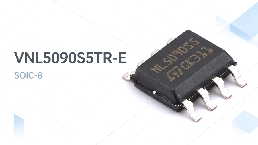
VNL5090S5TR-E Fully Protected Low-Side Driver IC
VNL5090S5TR-E is a monolithic fully protected low-side driver (Low-Side Driver / OMNIFET III) manufactured by STMicroelectronics using VIPower® M0-5 technology. It is specifically designed to drive resistive, inductive, or capacitive loads with one end connected to the battery. The device is AEC-Q100 automotive-qualified, uses a compact SOIC-8 (SO-8) package, provides a maximum continuous drain current of 13 A and a maximum on-resistance of 90 mΩ, and operates over a temperature range of -40°C to +150°C (junction temperature). It is a highly integrated solution for load driving and protection in automotive electronics and industrial control.
Compared with traditional discrete MOSFET + protection circuit solutions, the VNL5090S5TR-E integrates complete fault protection functions in a single chip, including overvoltage clamping, current limitation, power limitation, thermal shutdown, and open-load detection, and also features auto-restart capability—the device can immediately resume normal operation once the fault condition is removed. Its open-drain status output pin (unique to the VNL5090S5-E) can feed the chip's operating status back to the main controller in real time, greatly enhancing system maintainability and robustness. The device is officially positioned as a dedicated driver solution for 2×R10W or 4×R5W automotive signal lamps, and can also be widely used in motor drive, relay/solenoid control, and various in-vehicle load switch scenarios.
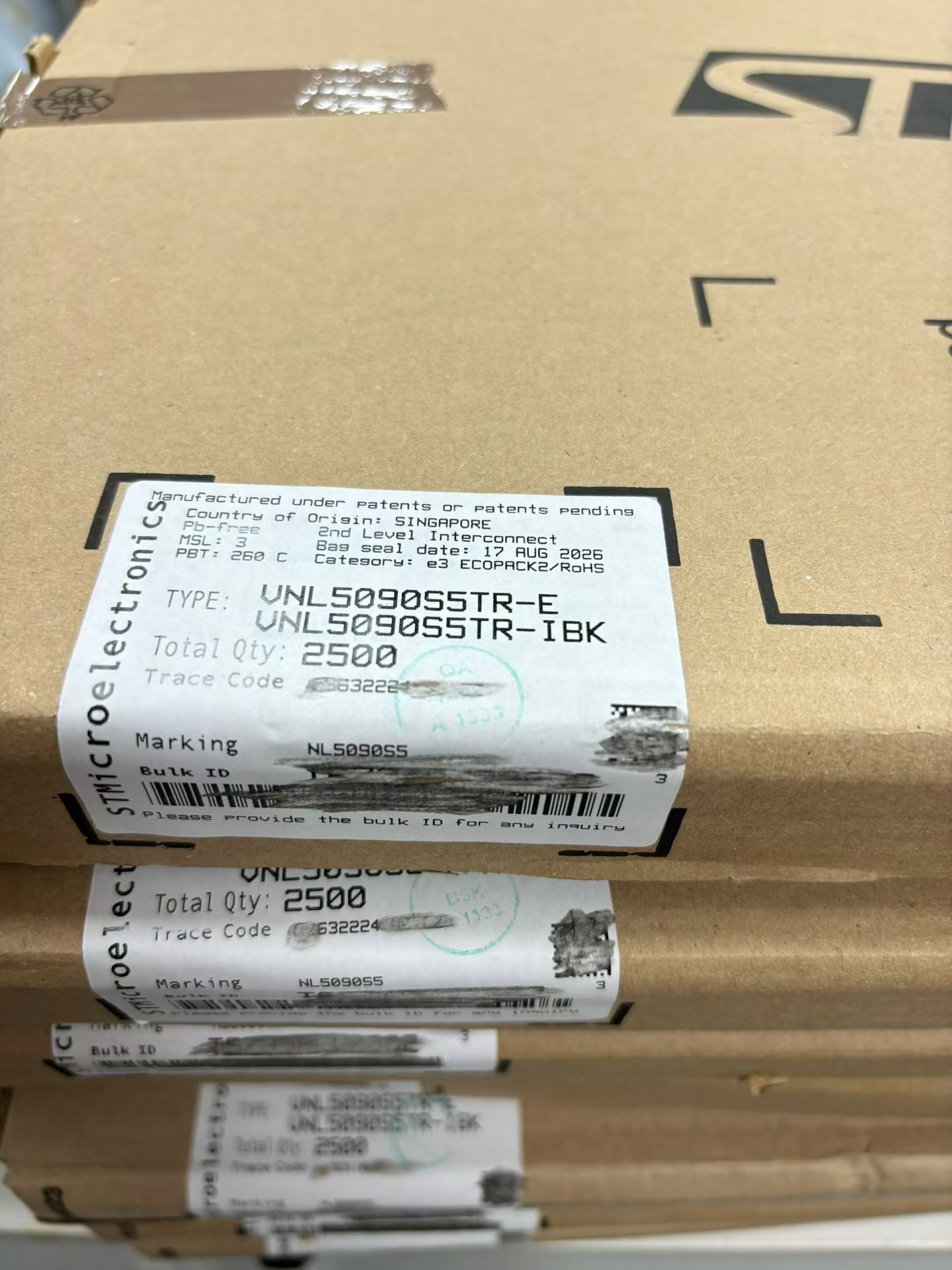
| Manufacturer | STMicroelectronics |
| Technology Platform | VIPower® M0-5 (OMNIFET III) |
| Device Type | Fully protected low-side driver (N-channel power MOSFET) |
| Package | SOIC-8 (SO-8, 3.90 mm body width) |
| Maximum Continuous Drain Current | 13 A |
| On-Resistance RDS(on) | 90 mΩ (maximum) |
| Load Voltage (Drain-Source) | 36 V (maximum) |
| Input Control Voltage (VIN) | 3.5 V to 5.5 V |
| Input Control Logic | Active high (non-inverting) |
| Number of Channels | 1 |
| Current Limit | 18 A (typical) |
| Operating Junction Temperature Range | -40°C to +150°C |
| Standby Current | Extremely low (25 µA typical) |
| Status Output | Open-drain output (Open Drain Status) |
| Fault Protection | Current limit (fixed), open-load detection, overtemperature protection, overvoltage protection |
| Special Features | Auto-restart, fast demagnetization |
Internal Structure and Operating Principle
The core of the VNL5090S5TR-E is an N-channel power MOSFET in a low-side configuration, meaning one end of the load is connected to the battery positive terminal (or power supply positive terminal), and the other end is connected to the device's drain (DRAIN), with the source (SOURCE) connected to ground. When a logic high level is applied to the input terminal (INPUT), the power MOSFET turns on and the load circuit is closed; when the input terminal is at a low level, the MOSFET turns off and the load is de-energized.
The chip internally integrates a gate drive circuit, current sensing and limiting circuit, temperature sensor, and status logic control unit. When overload or short circuit occurs, the current limiting function limits the output current to a safe level (typically 18 A); if the overload persists, the power limiting mechanism limits the dissipated power to a safe range until thermal shutdown intervenes; after thermal shutdown, the device enters an auto-restart cycle and automatically resumes conduction when the junction temperature drops below the safe threshold. In addition, when turning off inductive loads, the fast demagnetization function effectively suppresses reverse electromotive force spikes, protecting the internal MOSFET from overvoltage damage.
Key Features
Fully integrated protection. The chip integrates five protection mechanisms in a single package: overvoltage clamping, current limitation (18 A), power limitation, thermal shutdown, and open-load detection. Compared with protection circuits built from discrete components, the integrated solution significantly reduces BOM count, PCB area, and design complexity while improving system reliability.
Auto-restart. After thermal shutdown occurs, the chip does not permanently latch off but enters an auto-restart cycle—it automatically resumes conduction when the junction temperature drops below the safe threshold. This means transient overloads or brief short circuits will not cause permanent system failure, and the load driving function can automatically recover after the fault disappears.
Open-drain status output (S5 version only). The VNL5090S5TR-E provides an independent STATUS open-drain diagnostic pin that can feed the chip's fault status (such as overtemperature, open load, overvoltage) back to the main controller in real time. Developers can implement fault diagnosis and system protection strategies at the software level by reading the pin's logic level.
Extremely low electromagnetic susceptibility. The low electromagnetic susceptibility brought by VIPower technology makes the device very suitable for signal lamp control and load driving applications with strict EMC requirements in automotive electronic environments.
Ultra-low standby current. The typical standby current is only 25 µA, so in automotive "permanent live" scenarios (such as the standby state of a body control module), it does not place an additional burden on the battery.
AEC-Q100 automotive qualification. Passing AEC-Q100 certification means the device meets automotive-grade standards in reliability tests such as temperature cycling, high-temperature operating life, and ESD, and can be used directly in automotive electronic system designs.
Application Scenarios
Automotive signal lamp driving. This is the official core application scenario of the VNL5090S5TR-E. The device is specifically designed for 2×R10W or 4×R5W automotive signal lamps and can drive brake lights, turn signals, reverse lights, clearance lights, etc. Its 13 A current capability is sufficient to handle the load requirements of multiple lamps connected in parallel.
Automotive motor and actuator driving. In motor drive scenarios such as automotive seat adjustment, window lift, and power mirror folding, the VNL5090S5TR-E can serve as a low-side switch to control motor on/off. Its open-drain status output can be used to detect motor open-circuit (broken wire) faults, improving system diagnostic capability. Search results also show that the device is used in automotive electronic modules such as seat controllers and entry-level body control modules.
Relay and solenoid control. The device's built-in fast demagnetization function makes it very suitable for driving inductive loads. When a relay or solenoid is de-energized, the reverse electromotive force generated by the coil is quickly absorbed by the internal clamping circuit, allowing safe turn-off without an external freewheeling diode.
Industrial load switches and motor control. In addition to automotive applications, the device can also be used in industrial automation for load switches, small DC motor drives, solenoid control, and DC-DC converters. The high reliability brought by AEC-Q100 certification also makes it competitive in industrial environments.
Body electronic modules. In body electronic modules such as digital radios, infotainment systems, and instrument clusters, the VNL5090S5TR-E can be used to control power on/off for various loads.
FAQs
Q1: How should the STATUS open-drain output pin be correctly connected and used?
The STATUS pin is an open-drain output and must be externally pulled up to a logic supply (usually 3.3 V or 5 V) through a pull-up resistor (typical value 10 kΩ). When the device is operating normally, the STATUS pin is at a high level (pulled up by the pull-up resistor); when a fault is detected (overtemperature, open load, overvoltage, etc.), the internal open-drain transistor turns on and pulls the STATUS pin low. The main controller can determine the driver's status by reading the pin level. Note that the STATUS pin is provided only in the VNL5090S5-E version; the VNL5090N3-E (SOT-223 package) does not have this function. The value of the pull-up resistor must be a compromise based on the main controller's input leakage current and response speed requirements: too large a resistance reduces response speed, while too small a resistance increases power consumption in the fault state.
Q2: Can two VNL5090S5TR-E devices be connected in parallel to extend current capability?
Simple parallel connection is not recommended. The VNL5090S5TR-E is a fully protected intelligent driver with independent internal current limiting and thermal shutdown circuits. When two devices are connected in parallel, due to slight differences in on-resistance and threshold voltage, current sharing will be uneven—one device may trigger current limiting or thermal shutdown first while the other is still conducting normally, resulting in unpredictable system behavior. If greater current drive capability is truly required, it is recommended to choose a single-device solution with a higher current rating, or use a dedicated parallel current-sharing circuit. In scenarios where parallel connection is unavoidable, it is recommended to consult ST official technical support for specific current-sharing design guidance.
Q3: Is an external freewheeling diode required when driving inductive loads (relays/solenoids)?
Usually not required. The VNL5090S5TR-E has built-in overvoltage clamping and a fast demagnetization mechanism. When turning off an inductive load, the internal clamping circuit limits the drain voltage to a safe range, while the fast demagnetization function accelerates the decay of the coil current. However, in the following scenarios, it is still recommended to evaluate whether an external diode is needed: when the load inductance is extremely large (such as a large solenoid or contactor coil), the power dissipated by the internal clamp may exceed the chip's capability; when the turn-off frequency is extremely high, accumulated demagnetization energy may cause the junction temperature to rise. In these cases, a freewheeling diode can be connected in parallel with the load to share the demagnetization energy.
Q4: What are the key considerations for PCB layout?
As a power device, the PCB layout of the VNL5090S5TR-E significantly affects heat dissipation and reliability. Key points: The DRAIN pin (usually multiple pins connected in parallel) should be connected to a large copper area to enhance heat dissipation. It is recommended to lay heat-dissipating copper on both the top and bottom layers of the PCB and connect them through vias; the SOURCE pin should be grounded nearby, with the ground path as short and wide as possible; the INPUT and STATUS signal lines should be kept away from power traces to avoid switching noise coupling; the decoupling capacitor (100 nF recommended) should be placed close to the VIN pin. The thermal resistance Rth(j-amb) of the SOIC-8 package is approximately 60 to 80°C/W (depending on copper area). In high-current applications, the junction temperature must be calculated based on actual power dissipation to verify that it is within 150°C.
Q5: How can it be determined whether the device has entered thermal shutdown? What is the troubleshooting approach?
When the load does not work but the input signal is normal, troubleshoot as follows: First, measure the STATUS pin level—if it is low, the chip has detected a fault. Then use an oscilloscope to observe the voltage waveform at the OUTPUT (DRAIN) pin: if the voltage periodically jumps between 0 V and the load voltage, the chip is undergoing a thermal shutdown–auto-restart cycle, and the root cause is excessive load current or poor heat dissipation. Further troubleshooting directions include: confirm whether the load current exceeds the 13 A rating; check whether the copper area at the DRAIN pin is sufficient; if the load is inductive, confirm whether the demagnetization energy exceeds the chip's capability. If STATUS is high but the load does not work, the INPUT signal level may not meet the VIN requirement (3.5 V to 5.5 V), or the load itself may be open.
Conclusion
The VNL5090S5TR-E is a highly integrated fully protected low-side driver on STMicroelectronics' VIPower M0-5 platform. With a 13 A current capability, 90 mΩ on-resistance, and compact SOIC-8 package as its core, it integrates five protection mechanisms in a single chip—overvoltage clamping, current limitation, power limitation, thermal shutdown, and open-load detection—and provides two functions critical to system reliability: open-drain status output and auto-restart. AEC-Q100 automotive qualification and a wide junction temperature range of -40°C to +150°C give it significant advantages in automotive signal lamps, seat motors, relay/solenoid driving, and industrial load switches. In actual design, developers should focus on the STATUS pin pull-up resistor configuration, energy calculation for inductive load demagnetization, heat-dissipating copper design for the DRAIN pin, and fault diagnosis logic under thermal shutdown. With ST's official TwisterSIM electrothermal simulation tool, the device's thermal behavior can be simulated and verified during the design phase, thereby optimizing heat dissipation design and protection strategy.
Shenzhen Qixinwei Technology focuses on electronic component supply, BOM list, part matching, and supply chain solutions, and can assist in selecting corresponding products based on specific project requirements.
0users like this.