Electronic components
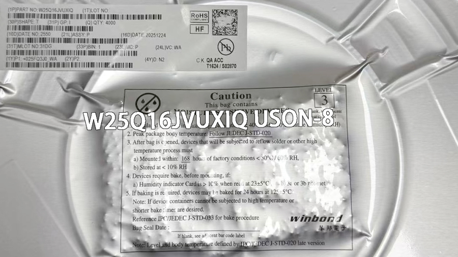
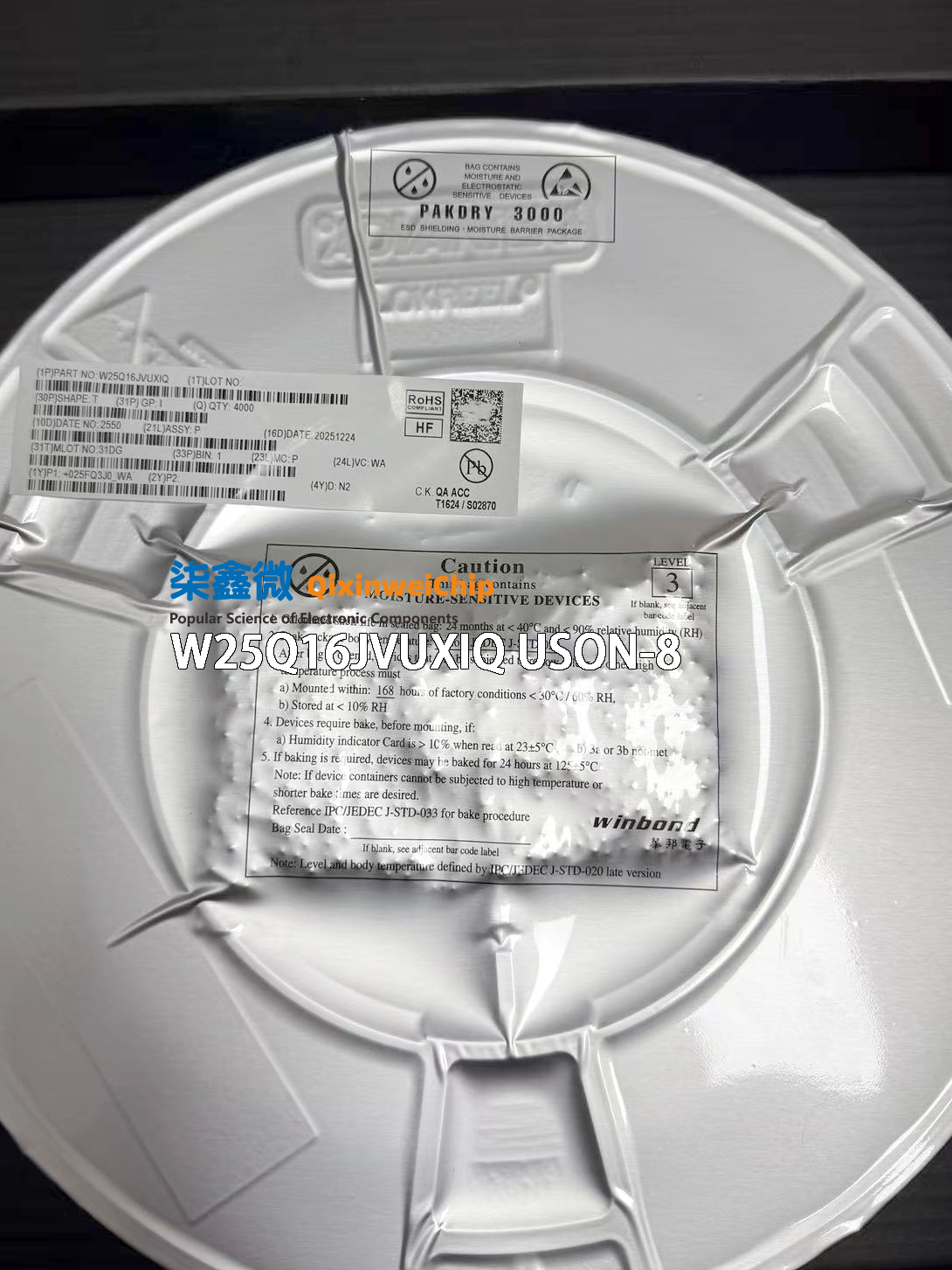
W25Q16JVUXIQ Analysis:16Mbit Serial NOR Flash IC
If you are picking a serial flash memory for a new embedded design, the first question is not “which density is largest” — it is “what does this memory actually have to survive.” A benchtop prototype with a generous SOIC-8 footprint looks fine on a schematic and falls apart the moment the board is a 10mm x 10mm wearable module, the power budget is measured in microamps, and the firmware needs to execute directly from flash without copying to RAM first. The W25Q16JVUXIQ from Winbond is a 16M-bit SpiFlash® memory that addresses all three constraints: a 2mm x 3mm USON-8 package, 1µA power-down current, and dual/quad SPI throughput at 133MHz.
What the W25Q16JVUXIQ is
The W25Q16JVUXIQ is a 16M-bit (2M-byte) Serial NOR Flash memory from Winbond’s SpiFlash® family, designed for systems with limited space, pins, and power. It operates on a single 2.7V to 3.6V supply with current consumption as low as 1µA in power-down. The array is organized into 8,192 programmable pages of 256 bytes each, supporting 4KB sector erase, 32KB block erase, 64KB block erase, and full chip erase — 512 erasable sectors and 32 erasable blocks in total. It supports standard SPI, Dual SPI, and Quad SPI operation with clock rates up to 133MHz (66MHz in DTR mode). The USON-8 package measures 2x3mm, making it one of the smallest 16Mb flash packages available. The part is rated for -40°C to +85°C operation with 100,000 program/erase cycles and 20-year data retention.
Core Specifications
| Series | W25Q |
| Memory Type | NOR Flash (non-volatile) |
| Memory Capacity | 16Mbit (2M bytes) |
| Organization | 2M × 8 |
| Interface Type | SPI, Dual SPI, Quad SPI |
| Maximum Clock Frequency | 133MHz |
| Quad SPI Equivalent Rate | 532MHz |
| Continuous Read Rate | Up to 66MB/s |
| Access Time | 6ns |
| Operating Voltage | 2.7V to 3.6V |
| Standby Current | 10µA |
| Sleep Current | 1µA maximum |
| Page Write Time | 3ms (typical) |
| Erase/Write Cycles | 100,000 (per sector) |
| Data Retention | 20 years |
| Operating Temperature | -40°C to +85°C |
| Package | USON-8-EP (2×3mm, 600µm height) |
| Memory Structure | 8,192 pages × 256 bytes |
| Erase Units | 4KB sector / 32KB block / 64KB block / full chip |
| Security Features | Software/hardware write protection, OTP protection, 64-bit unique serial number, 3 × 256-byte security registers |
Interface and Performance Features
The core competitiveness of the W25Q16JVUXIQ lies in its flexible SPI interface architecture. Standard SPI mode uses a single data input and output line and is compatible with all SPI hosts; Dual SPI mode expands the data lines to two (IO0 and IO1), doubling the equivalent transfer rate to 266MHz; Quad SPI mode further expands the data lines to four (IO0 to IO3), achieving an equivalent rate of 532MHz. This rate is already close to the bandwidth level of parallel NOR Flash, while the package pin count and PCB area are far smaller than parallel solutions.
The chip supports XIP (eXecute In Place), allowing the MCU to execute code directly from Flash via the Quad SPI interface without copying program code to RAM. For embedded systems with limited RAM resources (such as Cortex-M0+/M4-based solutions without external RAM), XIP can effectively free up valuable SRAM space for data caching and stack. With a 6ns access time and 133MHz clock, code execution efficiency in XIP mode can meet the needs of most real-time control applications.
Data Security and Protection Mechanisms
The W25Q16JVUXIQ provides a multi-level data protection scheme. Software write protection configures protected areas through the BP bits of the Status Register; hardware write protection is implemented through the WP pin, preventing accidental writes at the hardware level; OTP (one-time programmable) protection is used for permanent storage of security keys or calibration data. The chip also provides a 64-bit unique serial number and three 256-byte security registers, and supports JEDEC-standard manufacturer and device ID read commands (9Fh), facilitating system identification and anti-counterfeiting. These security features make the W25Q16JVUXIQ suitable for IoT terminals and industrial equipment requiring firmware protection, device identity authentication, and secure data storage.
Typical Application
Embedded system code storage. The W25Q16JVUXIQ is a classic choice for MCU external program storage. Its 2MB capacity can hold moderately complex firmware images, and the Quad SPI interface with XIP mode enables direct code execution, reducing dependence on external RAM. On MCU platforms such as the RP2040, this chip is widely used as external QSPI Flash.
Industrial control and smart instruments. The chip's wide operating temperature range (-40°C to +85°C) and 100,000 erase/write cycles make it suitable for industrial control boards, smart meters, data acquisition terminals, and other scenarios requiring frequent recording of operating parameters and configuration data.
Smart wearables and small sensor modules. The USON-8 (2×3mm) package occupies only 6mm², and its 600µm package height is suitable for ultra-thin devices. A sleep current as low as 1µA can significantly extend the battery life of battery-powered devices.
IoT terminals and OTA upgrades. The 2MB capacity provides ample temporary space for OTA firmware upgrades, supporting a dual-bank partitioning scheme (currently running firmware + firmware to be updated). Combined with security registers and a unique ID, it enables secure firmware verification and rollback.
Consumer electronics and home appliances. In consumer electronic products such as smart home appliances, set-top boxes, and audio equipment, the W25Q16JVUXIQ is used to store firmware, voice prompts, UI resource files, and user configuration data.
What the memory actually has to survive
A flash memory in a production embedded system is not a dev board on a desk. It is the component that stores the firmware, the configuration data, and often the entire application image. It has to hold up when the environment stops being friendly.
· Footprint pressure. The USON-8 2x3mm package is not a cosmetic choice. In wearables, hearables, and compact IoT modules, the PCB area allocated to memory is measured in square millimeters. A standard SOIC-8 occupies roughly 30mm²; the USON-8 2x3mm occupies 6mm². That 5x reduction is the difference between a board that fits the enclosure and one that does not.
· Power budget in battery-powered designs. The 1µA power-down current and 10µA standby current are the specifications that determine whether a coin-cell-powered device runs for months or years. The active read current of 25mA matters during firmware updates, but for most of the product’s life, the memory is in standby — and 10µA is a number that a power budget can live with.
· Execute-in-place (XIP) performance. The dual/quad SPI interfaces allow the host MCU to execute code directly from flash without copying to RAM. This is not just a convenience — it frees SRAM for the application, reduces boot time, and simplifies the memory architecture. The 133MHz clock rate provides 66MB/s in quad mode, which is fast enough for most Cortex-M4 and Cortex-M33 applications to run code from flash without a cache miss penalty.
· Write endurance and data retention. The 100,000 program/erase cycles and 20-year data retention are the specifications that determine whether the memory survives field updates, data logging, and configuration changes over the product’s lifetime. For applications that log sensor data or store calibration parameters, 4KB sector erase granularity provides flexibility without wearing out adjacent data.
· Industrial temperature range. The -40°C to +85°C operating range covers most industrial and consumer applications. Winbond also offers extended temperature grades (-40°C to +105°C and -40°C to +125°C) in the same series for designs that need more margin.
Where the W25Q16JVUXIQ fits — and where it doesn’t
The W25Q16JVUXIQ is the right choice when the design needs a small, low-power, high-performance flash memory for firmware storage, data logging, or execute-in-place operation. IoT sensors, wearables, hearables, smart home devices, portable medical monitors, industrial control boards, and automotive ECUs all fit.
It is the wrong choice when the design needs more than 16M-bit of storage — Winbond’s W25Q32JV (32M-bit) and W25Q64JV (64M-bit) provide higher densities in the same package family. It is also the wrong choice when the design needs NAND flash for high-capacity data storage, or when the host MCU lacks a SPI interface.
FAQs
Q1: SPI communication is normal, but the readback data is always shifted by one bit. How can this be troubleshooted?
This is one of the most common problems when using the W25Q series. The root cause is usually a mismatch in SPI mode configuration. The W25Q series supports SPI mode 0 (CPOL=0, CPHA=0) and mode 3 (CPOL=1, CPHA=1). Both sample data on the rising edge of the clock and update data on the falling edge. If the MCU is configured for mode 1 or mode 2 (sampling on the falling edge), the readback data will be shifted by one bit overall. Solution: Configure the MCU's SPI to mode 0 or mode 3; if the problem persists, use an oscilloscope to observe the CLK and DO signals simultaneously and confirm whether the sampling edge is aligned with the data valid window.
Q2: A write command has been issued, but the Flash still contains old data. How can this be solved?
Troubleshooting directions include three aspects. First, confirm whether the Write Enable (WREN, 06h) command is correctly sent before each write operation—the W25Q series requires the WREN command to be sent before every program or erase operation, otherwise the operation will be ignored. Second, check whether the WP pin and HOLD pin are at the correct logic levels—when WP is low, hardware write protection is active; when HOLD is low, communication is paused. These two pins must not be left floating or accidentally toggled during operation. Finally, confirm whether the polling mechanism after the write operation is correctly implemented—program operations require a typical time of 3ms. After sending the program command, the BUSY bit of the status register should be polled rather than reading immediately after a fixed delay.
Q3: How should Quad SPI mode be correctly configured to achieve maximum performance?
Enabling Quad SPI requires two steps. First, send the Quad Enable (QE) command (by writing the QE bit of Status Register 2) to enable Quad mode—this is the step most easily overlooked. If the QE bit is not enabled, IO2 and IO3 will remain in a high-impedance state, and Quad mode will not work. Second, use the Quad I/O Fast Read (EBh) instruction for data reading. This instruction transmits data over four IO lines after sending a 24-bit address. Performance optimization recommendations: In Quad mode, configure the SPI clock to 133MHz (confirm that the MCU's QSPI controller supports it); for XIP applications, enable the MCU's QSPI memory-mapped mode so that the Flash address space is directly mapped to the system address bus.
Q4: What alternative models are available for this chip?
In the same series, the W25Q16JVUXIM (similarity 86%) uses the same USON-8 package. The main difference is the operating temperature range, and it can serve as a cost-optimized option. The W25Q16RV is Winbond's new-generation R series (58nm process), officially recommended to replace the J series, but note that the R series differs in the write method of Status Register 2 and in some instruction timings. Design conversion should refer to the official application note. For cross-brand alternatives, the GD25Q16EEIGR (GigaDevice) and P25Q16SH-UXH-IR (Puya) are highly compatible in package and electrical parameters, with similarities of 79% and higher, respectively; the IS25LP016D-JULE-TR (ISSI) uses the same USON-8-EP (2×3mm) package and can be directly replaced with PCB compatibility.
0users like this.